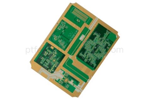
Kicad 7 multilayer pcb
Introduction To Multilayer PCB Design In Kicad 7
KiCad 7, the latest iteration of the popular open-source electronic design automation (EDA) software, has introduced a range of features that significantly enhance the process of designing multilayer printed circuit boards (PCBs). As electronic devices become increasingly complex, the demand for multilayer PCBs has grown, necessitating tools that can efficiently manage the intricacies involved in their design. KiCad 7 rises to this challenge by offering a suite of tools that streamline the design process, making it more accessible to both novice and experienced designers.
To begin with, KiCad 7 provides an intuitive interface that simplifies the initial setup of multilayer PCBs.
Users can easily define the number of layers required for their project, which is crucial for accommodating the various components and connections that modern electronic devices demand. This flexibility allows designers to tailor their PCBs to specific requirements, whether they are working on a simple four-layer board or a more complex design with ten or more layers. The software’s ability to handle such complexity is a testament to its robust architecture and user-centric design.
Moreover, KiCad 7 introduces enhanced layer management features that facilitate the organization and visualization of different layers within a PCB.
Designers can assign specific functions to each layer, such as power distribution, signal routing, or ground planes, ensuring that the board’s layout is both efficient and effective. The software’s layer stackup manager provides a clear overview of the board’s structure, allowing users to make informed decisions about layer placement and material selection. This level of control is essential for optimizing the board’s performance and ensuring signal integrity.
In addition to layer management, KiCad 7 offers advanced routing capabilities that are particularly beneficial for multilayer PCB design.
The software’s interactive router supports differential pair routing and length tuning, which are critical for maintaining signal integrity in high-speed designs. These features enable designers to create precise and reliable connections between components, reducing the risk of signal degradation and electromagnetic interference. Furthermore, the push-and-shove routing feature allows for dynamic adjustment of traces, making it easier to navigate complex layouts and avoid potential design conflicts.
Another noteworthy aspect of KiCad 7 is its comprehensive library of components and footprints, which is continually updated by a dedicated community of contributors.
This extensive library ensures that designers have access to a wide range of components, facilitating the integration of various elements into their multilayer PCBs. The software also supports custom footprint creation, allowing users to design unique components tailored to their specific needs. This flexibility is invaluable for projects that require specialized components or non-standard configurations.
Finally, KiCad 7’s simulation and analysis tools provide designers with the means to verify their designs before proceeding to fabrication.
By simulating the electrical behavior of the PCB, users can identify potential issues and make necessary adjustments, thereby reducing the likelihood of costly errors during production. The software’s integration with external simulation tools further enhances its analytical capabilities, offering a comprehensive solution for multilayer PCB design.
In conclusion, KiCad 7 represents a significant advancement in the field of EDA software, offering a powerful and versatile platform for designing multilayer PCBs. Its user-friendly interface, advanced routing features, extensive component library, and robust simulation tools make it an ideal choice for designers seeking to create complex electronic devices. As the demand for multilayer PCBs continues to grow, KiCad 7 stands out as a valuable resource for meeting the challenges of modern electronic design.
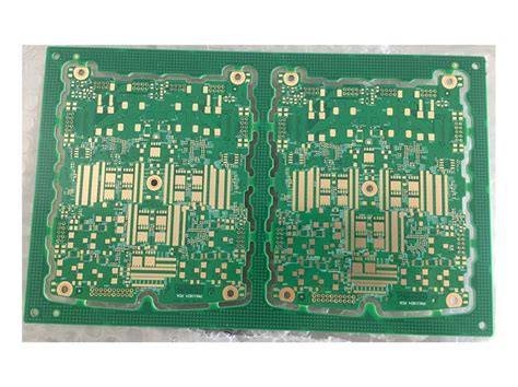
Advanced Routing Techniques For Multilayer PCBs In Kicad 7
In the realm of electronic design automation, KiCad 7 has emerged as a powerful tool for creating complex multilayer printed circuit boards (PCBs). As the demand for more compact and efficient electronic devices grows, the need for advanced routing techniques in multilayer PCBs becomes increasingly critical. KiCad 7 offers a suite of features that cater to these needs, enabling designers to optimize their PCB layouts effectively.
To begin with, understanding the fundamental structure of multilayer PCBs is essential.
These PCBs consist of multiple layers of conductive material separated by insulating layers, allowing for more intricate and compact designs. The additional layers provide more routing space, which is particularly beneficial for high-density designs. KiCad 7 supports the creation of PCBs with numerous layers, offering designers the flexibility to manage complex circuits with ease.
One of the key advanced routing techniques in KiCad 7 is the use of differential pair routing.
This technique is crucial for high-speed digital signals, where maintaining signal integrity is paramount. Differential pairs consist of two traces that carry equal and opposite signals, minimizing electromagnetic interference and crosstalk. KiCad 7 provides tools to define and route differential pairs, ensuring that the spacing and length matching are maintained throughout the design. This feature is particularly useful in applications such as USB, HDMI, and other high-speed communication interfaces.
Another significant feature in KiCad 7 is the support for blind and buried vias.
These vias are essential in multilayer PCBs as they allow connections between non-adjacent layers without passing through the entire board. Blind vias connect an outer layer to one or more inner layers, while buried vias connect only inner layers. The use of these vias can significantly reduce the complexity of routing and increase the available space for other components. KiCad 7’s interface allows designers to easily implement blind and buried vias, optimizing the board’s layout and performance.
Furthermore, KiCad 7 introduces enhanced support for impedance-controlled routing.
This is particularly important in RF and microwave applications, where maintaining a consistent impedance is crucial for signal integrity. The software allows designers to specify the desired impedance for specific traces and provides tools to adjust the trace width and spacing accordingly. This ensures that the PCB meets the necessary electrical specifications, reducing the risk of signal degradation.
In addition to these features, KiCad 7 offers improved design rule checks (DRC) and electrical rule checks (ERC).
These checks are vital for ensuring that the PCB design adheres to the specified constraints and standards. The DRC in KiCad 7 can be customized to accommodate the unique requirements of multilayer PCBs, such as minimum trace width, clearance, and via sizes. This level of customization helps prevent potential design errors and ensures that the final product is both reliable and manufacturable.
Moreover, KiCad 7’s user-friendly interface and extensive library of components make it accessible to both novice and experienced designers.
The software’s open-source nature encourages community contributions, resulting in a constantly evolving tool that adapts to the latest industry trends and technologies.
In conclusion, KiCad 7 provides a comprehensive set of features that facilitate advanced routing techniques for multilayer PCBs. By leveraging differential pair routing, blind and buried vias, impedance-controlled routing, and robust design rule checks, designers can create high-performance PCBs that meet the demands of modern electronic devices. As technology continues to advance, tools like KiCad 7 will play an increasingly important role in the development of innovative and efficient electronic solutions.
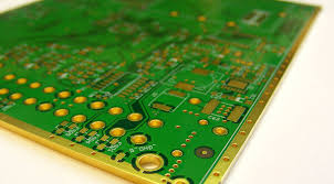
Managing Signal Integrity In Kicad 7 Multilayer PCB Designs
In the realm of electronic design automation, KiCad 7 has emerged as a powerful tool for creating multilayer printed circuit boards (PCBs). As electronic devices become increasingly complex, managing signal integrity in these designs is paramount. Signal integrity refers to the quality and reliability of electrical signals as they travel through a circuit. Poor signal integrity can lead to data errors, electromagnetic interference, and overall system instability. Therefore, understanding how to manage signal integrity in KiCad 7 multilayer PCB designs is crucial for engineers and designers.
One of the primary considerations in managing signal integrity is the stack-up configuration of the multilayer PCB.
The stack-up refers to the arrangement of conductive and insulating layers within the PCB. In KiCad 7, designers have the flexibility to define custom stack-ups, which is essential for optimizing signal paths and minimizing interference. By carefully selecting the number and order of layers, designers can create a balanced stack-up that supports high-speed signal transmission while reducing crosstalk and electromagnetic interference.
Moreover, the placement of components plays a significant role in signal integrity.
In KiCad 7, designers can utilize the software’s advanced layout tools to strategically position components, ensuring that critical signal paths are as short and direct as possible. This minimizes the potential for signal degradation and reduces the likelihood of interference from other components. Additionally, KiCad 7 allows for the implementation of ground planes, which are essential for providing a low-impedance return path for signals. Ground planes help to stabilize voltage levels and reduce noise, thereby enhancing signal integrity.
Transitioning to the routing of traces, it is imperative to consider trace width and spacing.
KiCad 7 offers precise control over these parameters, enabling designers to optimize trace dimensions for specific signal requirements. Wider traces can reduce resistance and inductance, which is beneficial for high-frequency signals. Meanwhile, maintaining adequate spacing between traces helps to prevent crosstalk, a phenomenon where signals in adjacent traces interfere with each other. By leveraging KiCad 7’s routing capabilities, designers can ensure that traces are routed efficiently and effectively, preserving signal integrity throughout the PCB.
Furthermore, the use of differential pairs is a common technique in managing signal integrity, especially for high-speed digital signals.
KiCad 7 supports the design and routing of differential pairs, which consist of two complementary signals that are routed together. This configuration helps to cancel out noise and electromagnetic interference, as any external disturbances affect both signals equally and are thus negated. By incorporating differential pairs into their designs, engineers can achieve robust signal integrity even in challenging environments.
In addition to these design strategies, simulation and analysis tools within KiCad 7 provide valuable insights into signal integrity.
Designers can perform simulations to predict how signals will behave under various conditions, allowing them to identify potential issues before physical prototyping. This proactive approach not only saves time and resources but also ensures that the final PCB design meets the desired performance criteria.
In conclusion, managing signal integrity in KiCad 7 multilayer PCB designs involves a comprehensive approach that encompasses stack-up configuration, component placement, trace routing, and the use of differential pairs. By leveraging the advanced features of KiCad 7, designers can create PCBs that maintain high signal quality and reliability, ultimately leading to more efficient and effective electronic devices. As technology continues to evolve, the importance of signal integrity in PCB design will only grow, making tools like KiCad 7 indispensable for modern engineers.
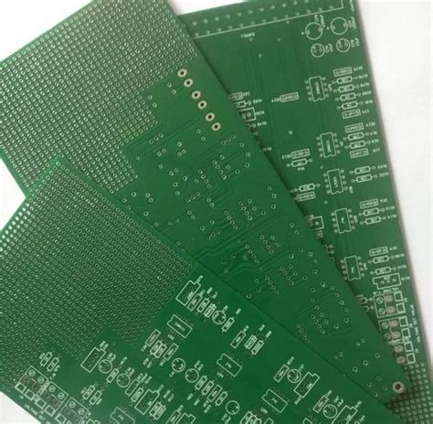
Best Practices For Layer Stackup In Kicad 7 Multilayer PCBs
When designing multilayer printed circuit boards (PCBs) in KiCad 7, understanding the best practices for layer stackup is crucial for achieving optimal performance and reliability. A well-considered layer stackup not only enhances the electrical performance of the PCB but also aids in thermal management and mechanical stability. As the complexity of electronic devices increases, the need for multilayer PCBs becomes more pronounced, making it essential for designers to master the intricacies of layer stackup.
To begin with, it is important to recognize the role of each layer in a multilayer PCB.
Typically, a multilayer PCB consists of signal layers, power planes, and ground planes. Signal layers are used for routing electrical connections, while power and ground planes provide stable voltage references and help in reducing electromagnetic interference (EMI). In KiCad 7, designers have the flexibility to define the number and type of layers based on the specific requirements of their project. However, it is advisable to maintain symmetry in the stackup to prevent warping during the manufacturing process.
One of the fundamental principles in layer stackup design is to place a ground plane adjacent to each signal layer.
This configuration minimizes the loop area for signal currents, thereby reducing EMI and crosstalk. Additionally, having a continuous ground plane helps in maintaining signal integrity by providing a low-impedance return path. In KiCad 7, designers can easily assign layers as ground planes and ensure they are strategically positioned within the stackup.
Another best practice is to use power and ground planes as a pair, sandwiching signal layers between them.
This arrangement, often referred to as a stripline configuration, offers excellent shielding for the signal traces and further reduces EMI. Moreover, it allows for controlled impedance routing, which is critical for high-speed digital and RF circuits. KiCad 7 provides tools for impedance calculation and trace width adjustment, enabling designers to achieve the desired electrical characteristics.
Thermal management is another critical aspect of multilayer PCB design.
By strategically placing power and ground planes, designers can create effective heat dissipation paths. Copper planes act as heat spreaders, distributing thermal energy across the board and preventing localized hotspots. In KiCad 7, thermal vias can be added to connect different layers, enhancing heat transfer and improving the overall thermal performance of the PCB.
Furthermore, it is essential to consider the manufacturability of the PCB when designing the layer stackup.
Factors such as the total number of layers, material selection, and layer thickness can impact the cost and feasibility of production. KiCad 7 allows designers to specify these parameters and provides a preview of the stackup, helping to ensure that the design is both functional and manufacturable.
In conclusion, mastering the best practices for layer stackup in KiCad 7 is vital for creating high-performance multilayer PCBs. By carefully considering the placement of signal, power, and ground layers, designers can optimize electrical performance, enhance thermal management, and ensure manufacturability. As electronic devices continue to evolve, the ability to design efficient multilayer PCBs will remain a valuable skill for engineers and designers alike. With KiCad 7’s robust features and user-friendly interface, achieving an optimal layer stackup is more accessible than ever, empowering designers to bring their innovative ideas to life.