KiCad: A Comprehensive Guide to Open-Source PCB Design
Introduction to KiCad
KiCad is a free and open-source software suite for electronic design automation (EDA). It facilitates the creation of printed circuit board (PCB) layouts and schematic diagrams for electronic circuits. Developed by Jean-Pierre Charras in 1992, KiCad has grown into a powerful tool used by hobbyists, engineers, and professionals worldwide. Unlike proprietary alternatives such as Altium Designer or Eagle, KiCad is completely free, with no restrictions on board size or layer count.
This article explores KiCad’s features, workflow, advantages, and limitations, providing a comprehensive guide for beginners and experienced users alike.
Key Features of KiCad
KiCad offers a robust set of features that make it a competitive choice for PCB design:
1. Cross-Platform Compatibility
KiCad runs on multiple operating systems, including Windows, macOS, and Linux. This flexibility allows users to work seamlessly across different environments.
2. Schematic Capture (Eeschema)
The schematic editor, Eeschema, allows users to design circuit diagrams with components, wires, and hierarchical sheets. Key functionalities include:
- Symbol library management
- Electrical rule checking (ERC)
- Netlist generation for PCB layout
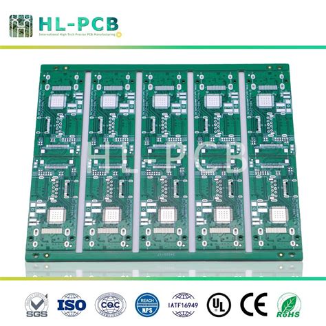
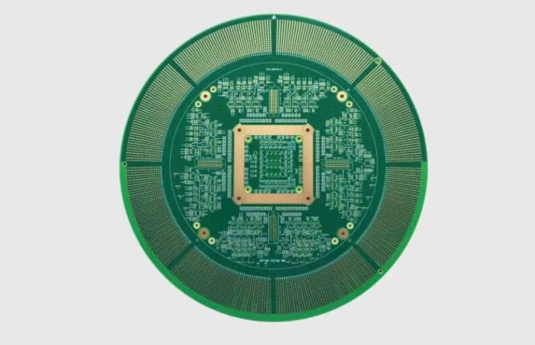
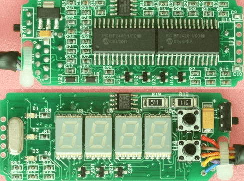
3. PCB Layout (Pcbnew)
Pcbnew is KiCad’s PCB layout editor, offering:
- Support for multi-layer PCBs (up to 32 layers)
- Interactive routing with push-and-shove features
- Design rule checking (DRC) to ensure manufacturability
- 3D viewer for visualizing the final board
4. Component Libraries
KiCad includes an extensive library of schematic symbols and PCB footprints. Users can also create custom components or import third-party libraries.
5. Gerber File Generation
KiCad exports industry-standard Gerber files for PCB manufacturing, along with drill files and pick-and-place data for assembly.
6. Integration with External Tools
KiCad supports scripting (Python) and can interface with simulation tools like SPICE for circuit analysis.

KiCad Workflow: From Schematic to PCB
Designing a PCB in KiCad follows a structured workflow:
Step 1: Schematic Design (Eeschema)
- Create a New Project: Start by setting up a project directory.
- Draw the Schematic: Place components from the library and connect them using wires.
- Annotate Components: Assign unique reference designators (e.g., R1, C2).
- Run ERC: Check for electrical errors like unconnected pins.
- Generate Netlist: Export the netlist for PCB layout.
Step 2: PCB Layout (Pcbnew)
- Import Netlist: Load the netlist to place components.
- Board Setup: Define board dimensions and layer stack-up.
- Component Placement: Arrange components for optimal routing.
- Routing: Manually or auto-route traces while adhering to design rules.
- Run DRC: Verify that the layout meets manufacturing constraints.
- Generate Output Files: Export Gerber, drill, and 3D model files.
Step 3: Manufacturing
Send the Gerber files to a PCB fabrication service. KiCad also supports generating BOM (Bill of Materials) for component procurement.
Advantages of Using KiCad
1. Free and Open-Source
Unlike proprietary tools that require expensive licenses, KiCad is completely free, making it accessible to students, hobbyists, and startups.
2. No Restrictions
KiCad does not impose limitations on board size, layer count, or commercial use—unlike some free versions of proprietary software.
3. Active Community Support
KiCad has a large user community and active development team. Forums, GitHub, and official documentation provide extensive support.
4. Regular Updates
The KiCad development team releases frequent updates, improving functionality and fixing bugs.
5. Customizable and Extensible
Users can create custom symbols, footprints, and scripts to enhance workflow efficiency.
Limitations of KiCad
Despite its strengths, KiCad has some drawbacks:
1. Steeper Learning Curve
Beginners may find KiCad’s interface less intuitive compared to some commercial tools.
2. Limited Advanced Features
While KiCad is powerful, it lacks some advanced features found in high-end EDA tools, such as advanced high-speed signal analysis.
3. Auto-Router Limitations
KiCad’s built-in auto-router is not as sophisticated as those in premium tools, often requiring manual adjustments.
4. Library Management Challenges
Although KiCad has extensive libraries, managing custom libraries can be cumbersome for large projects.
KiCad vs. Proprietary Alternative
| Feature | KiCad | Eagle (Free) | Altium Designer |
|---|---|---|---|
| Cost | Free | Limited free tier | Expensive |
| Layer Limit | 32 | 2 (Free) | Unlimited |
| Schematic Capture | Yes | Yes | Yes |
| 3D Viewer | Yes | Yes | Yes |
| Scripting | Python | Limited | Advanced |
| Community Support | Strong | Moderate | Professional |
KiCad is an excellent choice for those who need a full-featured PCB design tool without licensing costs. However, enterprises with complex design requirements might still prefer premium solutions like Altium.

Future of KiCad
KiCad continues to evolve with contributions from the open-source community. Future developments may include:
- Enhanced simulation integration
- Improved high-speed design tools
- Better collaboration features
- AI-assisted routing
As more users adopt KiCad, its capabilities will expand, potentially rivaling commercial EDA tools.
Conclusion
KiCad is a powerful, free, and open-source PCB design tool suitable for hobbyists, educators, and professionals. While it has some limitations, its active development and strong community support make it a compelling alternative to proprietary software. Whether you’re designing a simple Arduino shield or a complex multi-layer PCB, KiCad provides the tools needed to bring your electronic projects to life.
By mastering KiCad, users gain access to a versatile EDA platform without the financial burden of commercial software, fostering innovation in electronics design.