kicad-pcb
Introduction To KiCad-PCB: A Beginner’s Guide
KiCad-PCB is an open-source software suite for electronic design automation (EDA), which has gained significant popularity among hobbyists, educators, and professionals alike. It provides a comprehensive set of tools for designing electronic schematics and printed circuit boards (PCBs), making it an invaluable resource for anyone interested in electronics design. As a beginner’s guide, this article aims to introduce the fundamental aspects of KiCad-PCB, offering insights into its features and benefits, while also providing guidance on how to get started with this powerful tool.
To begin with, KiCad-PCB is renowned for its user-friendly interface, which is designed to accommodate both novice and experienced users.
The software is structured into several key components, each serving a specific purpose in the design process. These components include Eeschema for schematic capture, Pcbnew for PCB layout, and GerbView for viewing Gerber files, among others. This modular approach allows users to focus on individual aspects of their design, ensuring a streamlined workflow from concept to completion.
One of the most appealing features of KiCad-PCB is its open-source nature, which not only makes it freely available to users but also encourages community-driven development and support.
This collaborative environment has led to the continuous improvement of the software, with regular updates and enhancements being made available. Furthermore, the open-source model fosters a wealth of online resources, including tutorials, forums, and documentation, which can be invaluable for beginners seeking guidance and troubleshooting assistance.
In addition to its accessibility, KiCad-PCB offers a robust set of features that rival those of commercial EDA tools.
For instance, the software supports multi-layer PCB design, allowing users to create complex circuits with ease. It also includes a comprehensive library of components, which can be expanded with custom parts as needed. Moreover, KiCad-PCB’s design rule checking (DRC) and electrical rule checking (ERC) capabilities help ensure the accuracy and reliability of designs, reducing the likelihood of errors during the manufacturing process.
Transitioning from the theoretical aspects to practical application, getting started with KiCad-PCB involves a few straightforward steps.
Initially, users should download and install the software from the official KiCad website, ensuring they have the latest version for optimal performance. Once installed, it is advisable to familiarize oneself with the interface and basic functions through available tutorials and documentation. This foundational knowledge will prove beneficial as users embark on their first project.
When creating a new project in KiCad-PCB, the process typically begins with schematic capture in Eeschema.
Here, users can draw their circuit diagrams, placing components and connecting them with wires. This step is crucial, as it forms the blueprint for the subsequent PCB layout. After completing the schematic, users can proceed to Pcbnew, where they will arrange the physical layout of the PCB, positioning components and routing traces according to their design specifications.
As users gain experience with KiCad-PCB, they will likely discover additional features and techniques that enhance their design capabilities. For instance, the software’s 3D viewer provides a realistic representation of the finished PCB, allowing users to visualize their designs before fabrication. Additionally, KiCad-PCB’s integration with external tools and plugins can further extend its functionality, offering advanced options for simulation, analysis, and manufacturing.
In conclusion, KiCad-PCB stands out as a versatile and accessible tool for electronic design, offering a wealth of features and resources for beginners and experts alike. By understanding its core components and following a structured approach to design, users can harness the full potential of KiCad-PCB, bringing their electronic projects to life with precision and creativity.
Advanced Routing Techniques In KiCad-PCB
KiCad-PCB, an open-source software suite for electronic design automation, has become a popular choice among engineers and hobbyists for designing printed circuit boards (PCBs). As the complexity of electronic designs increases, mastering advanced routing techniques in KiCad-PCB becomes essential for ensuring optimal performance and reliability of the final product. This article delves into some of these advanced techniques, providing insights into how they can be effectively utilized to enhance PCB design.
To begin with, understanding the importance of trace width and spacing is crucial in advanced routing.
Trace width directly affects the current-carrying capacity of a PCB, while spacing impacts signal integrity and electromagnetic interference. KiCad-PCB offers tools to define design rules that ensure traces are routed with appropriate widths and clearances. By setting these parameters according to the specific requirements of the design, users can prevent issues such as overheating and crosstalk, which are common in densely packed circuits.
Transitioning to the topic of via management, it is important to note that vias are used to connect traces between different layers of a PCB.
In advanced routing, minimizing the number of vias is often desirable, as excessive use can lead to increased manufacturing costs and potential signal integrity issues. KiCad-PCB provides features such as blind and buried vias, which can be employed to optimize layer transitions without compromising the board’s performance. By strategically placing these vias, designers can maintain a clean and efficient layout.
Another critical aspect of advanced routing is the implementation of differential pairs.
Differential signaling is widely used in high-speed digital and RF designs to reduce noise and improve signal integrity. KiCad-PCB supports the routing of differential pairs by allowing users to define pairs of traces that must be routed together with controlled impedance. This feature ensures that the traces maintain consistent spacing and length, which is vital for minimizing skew and maintaining signal quality.
Furthermore, the use of copper pours and planes is an advanced technique that can significantly enhance the thermal and electrical performance of a PCB.
Copper pours are large areas of copper that can be used for power distribution or as ground planes. In KiCad-PCB, designers can easily create copper pours and assign them to specific nets, thereby reducing the impedance of power and ground connections. This not only improves the board’s thermal management but also helps in reducing electromagnetic interference by providing a return path for high-frequency signals.
In addition to these techniques, the concept of length matching is essential in advanced routing, particularly for high-speed designs.
Length matching ensures that signals traveling between components arrive simultaneously, which is critical for maintaining data integrity. KiCad-PCB offers tools to measure and adjust trace lengths, allowing designers to achieve precise length matching across multiple traces.
Finally, it is worth mentioning the role of design rule checks (DRC) in advanced routing.
DRCs are automated checks that verify whether a PCB design adheres to predefined rules and constraints. In KiCad-PCB, running DRCs can help identify potential routing issues early in the design process, enabling designers to make necessary adjustments before proceeding to fabrication.
In conclusion, mastering advanced routing techniques in KiCad-PCB is essential for creating high-performance and reliable PCBs. By understanding and applying concepts such as trace width and spacing, via management, differential pairs, copper pours, length matching, and design rule checks, designers can optimize their PCB layouts for both functionality and manufacturability. As electronic designs continue to evolve, these advanced techniques will remain integral to the success of PCB projects.
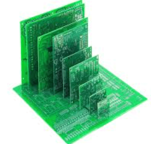
Designing Multi-Layer PCBs With KiCad-PCB
Designing multi-layer printed circuit boards (PCBs) is a complex task that requires precision, attention to detail, and a robust design tool. KiCad-PCB, an open-source software suite for electronic design automation (EDA), has emerged as a popular choice among engineers and hobbyists for creating sophisticated PCB layouts. This software provides a comprehensive set of features that facilitate the design of multi-layer PCBs, which are essential for modern electronic devices requiring compact and efficient circuitry.
To begin with, KiCad-PCB offers a user-friendly interface that simplifies the process of designing multi-layer PCBs.
The software allows users to create schematics, which serve as the blueprint for the PCB layout. By using the schematic editor, designers can easily place and connect components, ensuring that the electrical connections are accurate and efficient. This step is crucial, as it lays the foundation for the subsequent stages of the design process.
Once the schematic is complete, the next step involves transferring the design to the PCB layout editor.
KiCad-PCB excels in this area by providing a powerful layout editor that supports multiple layers. This feature is particularly important for multi-layer PCBs, as it allows designers to manage complex routing and component placement across several layers. The ability to work with multiple layers enables the creation of more compact and efficient designs, which are essential for high-performance electronic devices.
Moreover, KiCad-PCB includes a robust set of tools for managing design rules and constraints
These tools help ensure that the PCB design adheres to industry standards and best practices, which is critical for the reliability and functionality of the final product. By setting design rules, such as trace width and spacing, designers can prevent common issues like signal interference and crosstalk, which can compromise the performance of the PCB.
In addition to its design capabilities, KiCad-PCB offers advanced features for simulation and analysis.
The software integrates with SPICE, a widely used simulation tool, allowing designers to test their circuits before moving to the manufacturing stage. This integration is invaluable for identifying potential issues early in the design process, thereby reducing the risk of costly errors and rework. Furthermore, KiCad-PCB’s 3D viewer provides a realistic visualization of the PCB, enabling designers to inspect the layout from different angles and ensure that all components are correctly placed.
Transitioning from design to production, KiCad-PCB simplifies the process of generating manufacturing files.
The software supports the creation of Gerber files, which are the standard format used by PCB manufacturers. By providing accurate and detailed manufacturing files, KiCad-PCB ensures that the final product matches the designer’s specifications, thereby streamlining the production process.
In conclusion, KiCad-PCB is a powerful tool for designing multi-layer PCBs, offering a comprehensive suite of features that support every stage of the design process. From schematic creation to layout editing, rule management, simulation, and manufacturing file generation, KiCad-PCB provides the tools necessary to create high-quality, reliable PCBs. Its open-source nature and active community further enhance its appeal, making it an excellent choice for both professional engineers and hobbyists seeking to design complex electronic circuits. As technology continues to advance, the demand for efficient and compact PCB designs will only grow, and KiCad-PCB is well-positioned to meet these evolving needs.
Tips And Tricks For Efficient KiCad-PCB Workflow
KiCad-PCB, an open-source software suite for electronic design automation, has become a popular choice among engineers and hobbyists alike for designing printed circuit boards (PCBs). To maximize efficiency and productivity when using KiCad-PCB, it is essential to adopt certain tips and tricks that streamline the workflow. By implementing these strategies, users can enhance their design process, reduce errors, and ultimately produce high-quality PCBs.
To begin with, organizing your project files is crucial.
KiCad-PCB projects can quickly become complex, with numerous schematic sheets, PCB layouts, and libraries. Therefore, maintaining a well-structured directory system is vital. Create separate folders for schematics, layouts, libraries, and documentation. This organization not only simplifies navigation but also aids in version control, making it easier to track changes and collaborate with team members.
Another key aspect of an efficient workflow is mastering the use of keyboard shortcuts.
KiCad-PCB offers a wide array of shortcuts that can significantly speed up the design process. Familiarize yourself with these shortcuts, such as those for placing components, routing tracks, and switching between different views. By reducing reliance on mouse clicks, you can perform tasks more quickly and maintain a steady focus on the design.
In addition to shortcuts, customizing the KiCad-PCB interface to suit your preferences can greatly enhance productivity.
The software allows users to modify toolbars, panels, and color schemes. Tailor these elements to create a workspace that is comfortable and intuitive for you. For instance, placing frequently used tools within easy reach can save time and reduce frustration during complex design tasks.
Furthermore, leveraging KiCad-PCB’s extensive library management capabilities is essential for efficient component handling.
The software includes a vast collection of pre-defined components, but creating custom libraries for frequently used parts can save time in the long run. By organizing components into logical categories and ensuring that each part has accurate footprints and symbols, you can minimize errors during the design phase. Additionally, regularly updating libraries to include new components or revisions ensures that your designs remain current and reliable.
Transitioning from schematic design to PCB layout is a critical step in the workflow.
To facilitate this process, ensure that your schematic is meticulously checked for errors before proceeding. KiCad-PCB provides an Electrical Rules Check (ERC) tool that identifies common issues such as unconnected pins or mismatched net names. Addressing these errors early on prevents complications during the layout phase and reduces the likelihood of costly revisions later.
Once the PCB layout begins, employing design rules and constraints is vital for maintaining quality and manufacturability.
KiCad-PCB allows users to define specific design rules, such as minimum trace widths, clearance distances, and via sizes. By adhering to these rules, you can ensure that your design meets industry standards and is compatible with manufacturing processes. Moreover, utilizing the Design Rule Check (DRC) tool throughout the layout process helps identify violations and rectify them promptly.
Finally, taking advantage of KiCad-PCB’s 3D visualization capabilities can provide valuable insights into the final product.
By viewing the PCB in three dimensions, you can verify component placements, check for potential mechanical conflicts, and gain a better understanding of the overall design. This visualization aids in identifying issues that may not be apparent in a two-dimensional view, ultimately leading to a more robust and reliable PCB.
In conclusion, optimizing your KiCad-PCB workflow involves a combination of organization, customization, and adherence to best practices. By implementing these tips and tricks, users can enhance their design efficiency, reduce errors, and produce high-quality PCBs that meet their project requirements.


