Kicad rf pcb
Designing RF PCBs with KiCad: Best Practices and Tips
Designing RF PCBs with KiCad requires a meticulous approach, as radio frequency circuits demand precision and careful consideration of various factors to ensure optimal performance. KiCad, an open-source PCB design tool, offers a robust platform for creating RF circuits, but it is essential to follow best practices to achieve the desired results. To begin with, understanding the fundamental principles of RF design is crucial. RF circuits operate at high frequencies, where even the smallest parasitic elements can significantly impact performance. Therefore, designers must pay close attention to component placement, trace routing, and grounding techniques.
One of the first steps in designing RF PCBs with KiCad is to carefully select the components.
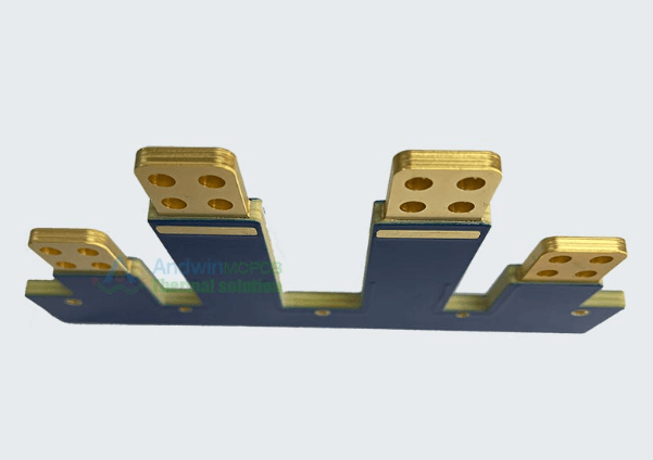
RF components, such as inductors, capacitors, and transistors, should be chosen based on their frequency response and quality factor. It is advisable to use components specifically designed for RF applications to minimize losses and ensure stability. Once the components are selected, the next step is to create a schematic in KiCad. This involves placing the components and defining their connections. It is important to keep the schematic organized and to use clear labeling to avoid confusion during the layout phase.
Transitioning from schematic to layout, the placement of components on the PCB is a critical aspect of RF design.
Components should be placed to minimize the length of signal paths, thereby reducing inductance and resistance. Additionally, sensitive components should be isolated from noisy elements to prevent interference. KiCad provides tools to assist with component placement, allowing designers to experiment with different configurations to achieve the best layout.
Routing traces in RF PCBs is another area where precision is paramount.
Traces should be kept as short and direct as possible to minimize signal loss and reflections. It is also essential to maintain consistent trace widths and spacing to ensure impedance matching, which is vital for RF signal integrity. KiCad’s design rules can be configured to enforce these constraints, helping designers maintain control over the routing process.
Grounding is a fundamental aspect of RF PCB design, as it affects the overall performance and stability of the circuit.
A solid ground plane is recommended to provide a low-impedance path for return currents and to shield sensitive components from electromagnetic interference. KiCad allows designers to define ground planes and vias, facilitating the creation of an effective grounding strategy.
Moreover, the use of simulation tools can greatly enhance the design process.
KiCad integrates with various simulation software, enabling designers to model and analyze their RF circuits before fabrication. This step is invaluable for identifying potential issues and optimizing the design for performance.
Finally, it is important to consider the manufacturing process when designing RF PCBs with KiCad.
Factors such as board material, layer count, and fabrication tolerances can influence the final performance of the circuit. Collaborating with manufacturers early in the design process can help ensure that the PCB is manufacturable and meets the desired specifications.
In conclusion, designing RF PCBs with KiCad involves a combination of careful planning, precise execution, and thorough testing. By adhering to best practices in component selection, layout, routing, grounding, and simulation, designers can create high-performance RF circuits that meet their specific requirements. KiCad’s comprehensive toolset provides the necessary capabilities to tackle the challenges of RF design, making it a valuable resource for engineers in this specialized field.
Advanced Techniques for RF Circuit Simulation in KiCad
KiCad, an open-source electronic design automation (EDA) tool, has gained significant traction among engineers and hobbyists for its robust capabilities in designing printed circuit boards (PCBs). When it comes to radio frequency (RF) circuit simulation, KiCad offers a suite of advanced techniques that can be leveraged to optimize the design and functionality of RF PCBs. Understanding these techniques is crucial for engineers aiming to achieve high performance in RF applications.
To begin with, the integration of KiCad with external simulation tools is a pivotal aspect of RF circuit design.
While KiCad itself does not include a built-in RF simulator, it can be seamlessly paired with powerful simulation software such as SPICE or QUCS. This integration allows designers to perform detailed analyses of RF circuits, including S-parameter simulations, which are essential for understanding how RF signals propagate through the circuit. By exporting the schematic from KiCad and importing it into these simulation tools, engineers can evaluate the performance of their designs under various conditions, thereby ensuring that the final product meets the desired specifications.
Moreover, the layout of RF PCBs in KiCad requires meticulous attention to detail.
RF circuits are highly sensitive to parasitic elements such as inductance and capacitance, which can significantly affect performance. Therefore, employing advanced layout techniques is imperative. For instance, maintaining consistent trace widths and minimizing the length of signal paths can reduce unwanted inductive and capacitive effects. Additionally, the use of ground planes and proper via placement can help in managing electromagnetic interference (EMI), which is a common challenge in RF designs. KiCad’s PCB editor provides the necessary tools to implement these techniques, allowing designers to create efficient and reliable RF circuits.
Transitioning from layout to component selection, it is important to note that the choice of components plays a critical role in RF circuit performance.
Components such as capacitors, inductors, and resistors must be selected with precision, considering their frequency response and quality factor (Q-factor). KiCad’s extensive library of components, along with the ability to import custom libraries, facilitates the selection of suitable components for RF applications. Furthermore, the use of simulation models provided by component manufacturers can enhance the accuracy of simulations, leading to more reliable designs.
In addition to component selection, impedance matching is another crucial aspect of RF circuit design.
Proper impedance matching ensures maximum power transfer between different stages of the circuit, minimizing signal reflection and loss. KiCad, in conjunction with external simulation tools, allows designers to calculate and optimize impedance matching networks. By simulating various matching network configurations, engineers can identify the most effective design for their specific application.
Finally, the iterative nature of RF circuit design necessitates a thorough validation process.
After initial simulations and layout, prototyping and testing are essential to verify the performance of the RF PCB. KiCad’s ability to generate Gerber files and other manufacturing outputs streamlines the transition from design to production, enabling rapid prototyping and testing. By iterating on the design based on test results, engineers can refine their RF circuits to achieve optimal performance.
In conclusion, KiCad offers a comprehensive platform for RF PCB design when combined with external simulation tools and advanced design techniques. By focusing on integration, layout, component selection, impedance matching, and validation, engineers can effectively utilize KiCad to develop high-performance RF circuits. As the demand for RF applications continues to grow, mastering these advanced techniques in KiCad will be invaluable for engineers seeking to excel in the field of RF design.
KiCad vs. Other EDA Tools for RF PCB Design: A Comparative Analysis
In the realm of electronic design automation (EDA) tools, KiCad has emerged as a formidable contender, particularly in the niche of radio frequency (RF) printed circuit board (PCB) design. As engineers and designers seek efficient and cost-effective solutions, the comparison between KiCad and other EDA tools becomes increasingly pertinent. This analysis aims to elucidate the advantages and limitations of KiCad in comparison to its competitors, thereby providing a comprehensive understanding of its suitability for RF PCB design.
To begin with, KiCad is an open-source EDA tool that has gained significant traction due to its cost-effectiveness and robust feature set.
Unlike proprietary software, KiCad offers a free platform that is continuously improved by a community of developers. This aspect is particularly appealing to small businesses and individual designers who may not have the budget for expensive licenses. In contrast, other EDA tools such as Altium Designer and Cadence Allegro, while offering advanced features, come with substantial costs that can be prohibitive for some users.
Transitioning to the technical capabilities, KiCad provides a comprehensive suite of tools for schematic capture, PCB layout, and 3D visualization.
For RF PCB design, the ability to handle complex layouts and high-frequency signals is crucial. KiCad supports multi-layer boards and offers a range of features such as differential pair routing and length tuning, which are essential for RF applications. However, it is important to note that while KiCad’s capabilities are impressive, they may not match the advanced simulation and analysis features found in high-end tools like Keysight ADS or Ansys HFSS, which are specifically tailored for RF design.
Moreover, the user interface and ease of use are critical factors in the selection of an EDA tool.
KiCad’s interface is intuitive and user-friendly, making it accessible to both novice and experienced designers. The tool’s modular design allows users to customize their workflow, which can enhance productivity. On the other hand, some proprietary tools offer more polished interfaces and integrated environments that streamline the design process, albeit at a higher cost.
Another aspect to consider is the support and community surrounding the EDA tool.
KiCad benefits from a vibrant community that contributes to its development and provides extensive documentation and tutorials. This community-driven support can be invaluable for troubleshooting and learning. In contrast, proprietary tools often offer professional customer support and training, which can be advantageous for large organizations that require reliable assistance.
In terms of interoperability, KiCad supports a variety of file formats, allowing for seamless integration with other tools and systems.
This flexibility is beneficial for designers who need to collaborate with others using different software. However, some proprietary tools offer more comprehensive integration with other design and simulation software, which can be a deciding factor for complex projects.
In conclusion, KiCad presents a compelling option for RF PCB design, particularly for those who prioritize cost-effectiveness and flexibility. While it may not offer the same level of advanced features and professional support as some proprietary tools, its open-source nature and active community make it a viable choice for many designers. Ultimately, the decision between KiCad and other EDA tools will depend on the specific needs and constraints of the project at hand.
Optimizing RF PCB Layouts in KiCad for Enhanced Performance
Optimizing RF PCB layouts in KiCad for enhanced performance requires a meticulous approach, as the intricacies of radio frequency design demand precision and attention to detail. KiCad, an open-source electronic design automation tool, offers a robust platform for designing RF PCBs, but achieving optimal performance necessitates a deep understanding of both the software and the principles of RF design. To begin with, it is essential to recognize that RF circuits are highly sensitive to layout configurations. Therefore, the placement of components and the routing of traces must be executed with precision to minimize interference and signal loss.
One of the primary considerations in RF PCB design is the impedance matching of transmission lines.
In KiCad, designers can utilize the integrated tools to calculate and adjust trace widths to achieve the desired impedance. This is crucial for maintaining signal integrity and minimizing reflections, which can degrade performance. Additionally, the use of ground planes is vital in RF designs to provide a return path for signals and to shield sensitive components from electromagnetic interference. KiCad allows for the easy creation and manipulation of ground planes, enabling designers to effectively manage these aspects.
Moreover, the layout of RF components should be approached with a strategy that minimizes parasitic capacitance and inductance.
+This involves careful placement of components such as capacitors and inductors, ensuring they are positioned close to the ICs they support. KiCad’s layout editor facilitates this by allowing precise control over component placement and trace routing. Furthermore, the use of vias should be minimized in RF designs, as they can introduce unwanted inductance. When vias are necessary, they should be strategically placed and kept as short as possible.
Transitioning to the topic of signal isolation, it is imperative to separate RF signals from digital signals to prevent crosstalk and interference. KiCad provides the capability to define separate zones for different signal types, which can be used to isolate RF circuits from other parts of the PCB. This separation is crucial for maintaining the integrity of RF signals and ensuring reliable performance. Additionally, the use of shielding techniques, such as placing RF components within a grounded enclosure, can further enhance isolation.
Thermal management is another critical aspect of RF PCB design.
High-frequency components can generate significant heat, which can affect performance and reliability. KiCad’s thermal simulation tools can be employed to analyze heat distribution and identify potential hotspots. By incorporating thermal vias and heat sinks into the design, designers can effectively manage heat dissipation and maintain optimal operating conditions.
In conclusion, optimizing RF PCB layouts in KiCad for enhanced performance involves a comprehensive understanding of RF design principles and the effective use of KiCad’s features. By focusing on impedance matching, minimizing parasitic effects, ensuring signal isolation, and managing thermal issues, designers can create RF PCBs that deliver superior performance. The open-source nature of KiCad, combined with its powerful design tools, makes it an excellent choice for engineers seeking to develop high-quality RF circuits. As technology continues to advance, the ability to optimize RF PCB layouts will remain a critical skill for achieving success in the field of electronics design.