Layer PCB Manufacturer: Ensuring Quality and Efficiency

Key Takeaways
When evaluating PCB manufacturing partners for 6-layer designs, you’ll want to prioritize high-density capabilities and advanced processes like Via-in-Pad technology, which minimizes signal loss in compact layouts. Reputable PCB manufacturing companies leverage 4-wire testing to ensure electrical integrity, reducing defects in applications like wearables or industrial systems where reliability is non-negotiable.
Balancing PCB manufacturing cost with performance requires expertise in stack-up optimization—proper layer arrangement enhances signal integrity while avoiding unnecessary material waste. For time-sensitive projects, some providers offer 48-hour turnaround without compromising on testing rigor, a critical advantage in fast-paced PCB manufacturing business environments.
By aligning your design requirements with a manufacturer’s technical strengths—whether for industrial-grade thermal management or wearable-grade miniaturization—you ensure both quality and efficiency. Transitioning between prototyping and mass production becomes seamless when your partner integrates design feedback early, addressing potential bottlenecks in PCB manufacturing workflows before they escalate.

High-Density 6-Layer PCB Manufacturing
When designing compact electronics like wearables or industrial control systems, PCB manufacturing must balance density with reliability. High-density 6-layer PCBs achieve this through advanced stacking techniques and precision engineering. These boards often incorporate Via-in-Pad technology, which reduces signal path lengths while maintaining thermal stability—a critical factor for devices operating in extreme environments.
Leading PCB manufacturing companies prioritize material selection and layer alignment to minimize crosstalk and impedance mismatches. For example, a typical stack-up might pair power and ground layers adjacent to high-speed signal layers, optimizing electromagnetic performance. To ensure quality, rigorous 4-wire testing verifies electrical continuity and isolation, catching defects early in production.
| Feature | High-Density 6-Layer PCB | Standard 6-Layer PCB |
|---|---|---|
| Trace Width/Spacing | ≤3 mil | ≥5 mil |
| Via Type | Microvia & Blind/Buried | Through-Hole Only |
| Testing Method | 4-Wire Kelvin | 2-Wire |
| Typical Application | Medical Sensors | Consumer Electronics |
Understanding PCB manufacturing cost drivers—such as material grades, layer complexity, and testing protocols—helps you budget effectively. For industrial electronics applications, advanced manufacturing techniques ensure durability without inflating expenses. Whether scaling a PCB manufacturing business or prototyping a niche product, partnering with specialists who offer rapid turnaround times ensures your projects stay on schedule without compromising performance.
Via-in-Pad Technology Benefits Explained
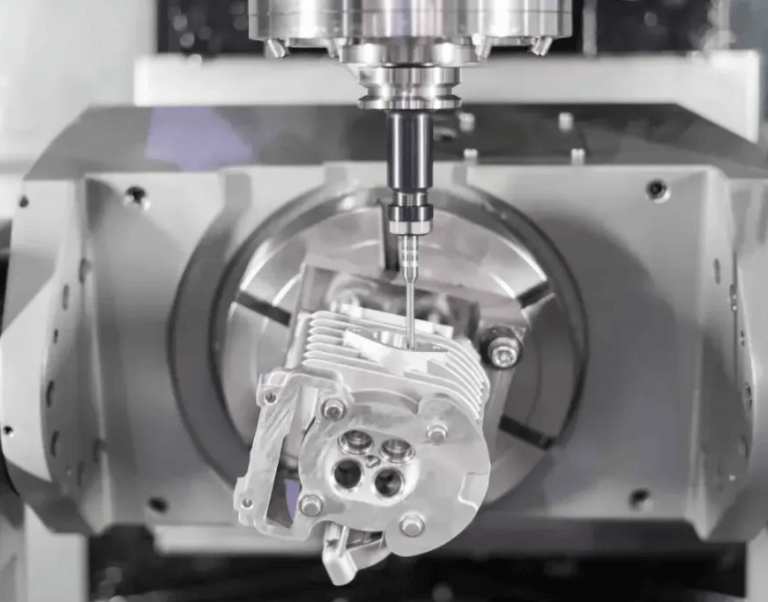
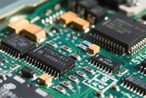
When designing complex multilayer boards, PCB manufacturing companies leverage via-in-pad technology to address spatial constraints while maintaining signal integrity. This method embeds vias directly into component pads, eliminating the need for separate routing channels—a critical advantage for high-density PCB manufacturing in wearables or industrial systems. By reducing trace lengths, you minimize impedance mismatches and improve thermal dissipation, ensuring stable performance in compact devices.
For PCB manufacturing cost optimization, this technique streamlines production by reducing layer counts and material waste. Traditional designs often require additional layers to route connections around pads, but via-in-pad integration allows tighter component placement. This efficiency not only lowers material expenses but also accelerates assembly cycles—key for PCB manufacturing business models prioritizing rapid turnaround.
However, precise laser drilling and advanced plating processes are essential to avoid voids or reliability issues. Reputable manufacturers combine this technology with rigorous testing protocols, ensuring robust interconnects even in demanding environments. By adopting via-in-pad solutions, you achieve a balance between miniaturization and durability, critical for next-generation electronics requiring both performance and space efficiency.

4-Wire Testing for Quality Assurance
When evaluating PCB manufacturing processes, 4-wire testing stands as a critical method for ensuring electrical integrity in multilayer designs. Unlike traditional 2-wire testing, this approach eliminates lead resistance errors by separating current injection and voltage measurement paths. For PCB manufacturing companies, adopting this technique reduces false failures and guarantees traceable accuracy in high-density circuits—especially vital for applications like wearables or industrial systems where signal reliability is non-negotiable.
You’ll find that integrating 4-wire testing directly impacts PCB manufacturing cost by minimizing rework and material waste. While initial setup might require specialized equipment, the long-term savings from reduced defect rates justify the investment. Leading manufacturers pair this method with automated optical inspection (AOI) to cross-verify impedance values and via continuity, creating a multi-layered quality framework.
For your PCB manufacturing business, prioritizing such precision-driven protocols strengthens client trust and compliance with industry standards like IPC-6012. Whether prototyping or scaling production, 4-wire testing ensures every layer in a 6-layer stack-up meets exact specifications—critical for maintaining performance in thermally demanding environments. This focus on uncompromised quality aligns with broader goals of balancing speed and reliability in complex board fabrication.

Fast 48-Hour Turnaround Solutions
When selecting a PCB manufacturing partner, speed often becomes a critical component of project success. Leading PCB manufacturing companies now leverage automated production lines and real-time monitoring systems to deliver complex 6-layer boards within 48 hours. This accelerated process doesn’t compromise quality—advanced machinery ensures precise layer alignment, while rigorous testing protocols maintain reliability standards.
For time-sensitive industries like wearables or IoT devices, rapid turnaround directly impacts time-to-market. By integrating lean workflows and predictive logistics, manufacturers reduce idle periods between design approval and production. This efficiency also helps manage PCB manufacturing cost, as optimized material usage and reduced waste lower overall expenses.
However, achieving this speed requires expertise. Trusted providers balance accelerated timelines with thorough design validation, ensuring your PCB manufacturing business avoids costly revisions. Precisely calibrated equipment handles high-density interconnects and via-in-pad placements without delays, while 4-wire testing guarantees electrical performance. Unlike traditional approaches, modern solutions prioritize both velocity and precision, making 48-hour delivery a non-negotiable advantage in competitive markets.

Wearable Electronics PCB Specifications
When designing PCB manufacturing solutions for wearable devices, you face unique challenges that demand precision engineering. These compact electronics require high-density interconnect (HDI) layouts to accommodate shrinking form factors while maintaining signal integrity. Leading PCB manufacturing companies prioritize 6-layer stack-ups to balance space constraints with thermal management, ensuring reliable performance in body-worn applications.
Critical specifications include flexible substrates for ergonomic designs and Via-in-Pad technology to minimize layer transitions—key for reducing impedance variations in high-frequency sensors. To maintain durability, manufacturers employ 4-wire Kelvin testing to verify solder joint reliability under repeated mechanical stress. Such rigorous quality protocols directly impact PCB manufacturing cost, but they’re non-negotiable for wearables exposed to moisture, temperature swings, and physical strain.
Optimizing PCB manufacturing business workflows for wearables also involves material selection, with polyimide-based laminates favored for their heat resistance and bend endurance. By aligning design choices with scalable production methods, you ensure faster prototyping cycles without compromising the stringent standards demanded by medical trackers, smartwatches, or fitness monitors.
Industrial-Grade Multilayer PCB Design
When designing industrial-grade multilayer PCBs, you need to prioritize durability and reliability to withstand harsh operating environments. Unlike consumer electronics, industrial applications demand boards capable of handling extreme temperatures, vibrations, and prolonged operational cycles. Thermal management becomes critical here, requiring careful material selection—such as high-Tg laminates or metal-core substrates—to prevent delamination or warping under stress.
Leading PCB manufacturing companies optimize layer stack-ups to balance signal integrity and mechanical stability. For instance, placing power and ground planes adjacent to critical signal layers minimizes electromagnetic interference (EMI), a common challenge in industrial systems. Advanced PCB manufacturing techniques like controlled impedance routing and via shielding further enhance performance in high-noise settings.
Cost considerations in PCB manufacturing business models often lead to trade-offs between material quality and production efficiency. However, cutting corners on layer alignment or copper thickness risks premature failure in mission-critical equipment. Partnering with manufacturers that offer rigorous testing protocols (like 4-wire Kelvin testing) ensures consistent quality without inflating PCB manufacturing cost. By aligning design choices with industrial requirements, you create robust boards that meet both technical specifications and long-term operational demands.
Optimizing 6-Layer Stack-Up Configurations
When designing a 6-layer PCB, the stack-up configuration directly impacts signal integrity, power distribution, and thermal performance. A well-optimized stack-up balances impedance control and EMI shielding while minimizing PCB manufacturing cost. For high-density designs common in wearables or industrial electronics, typical configurations include two signal layers, two ground planes, and two power planes. Placing high-speed signal layers adjacent to ground planes reduces crosstalk, while dedicated power planes ensure stable voltage delivery—critical for devices requiring 4-wire testing accuracy.
Collaborating with experienced PCB manufacturing companies ensures material selection aligns with your application’s demands. For example, using low-loss laminates (e.g., FR-4 or high-frequency substrates) improves signal integrity in RF-heavy designs. Proper via placement, such as via-in-pad technology, further enhances routing efficiency without compromising layer spacing. This is especially vital for compact wearables where space constraints demand precision.
Thermal management is another key consideration. Thicker copper layers or thermal vias can dissipate heat effectively, extending component lifespan in industrial environments. By optimizing layer ordering and material choices early, you streamline the PCB manufacturing business workflow, avoiding costly redesigns. Whether prioritizing speed (e.g., 48-hour turnaround) or durability, a strategic stack-up ensures your design meets both performance benchmarks and budget requirements.
Cost-Effective 6-Layer PCB Production
Achieving cost efficiency in PCB manufacturing requires balancing advanced engineering with strategic material and process choices. When selecting PCB manufacturing companies, prioritize those that integrate design for manufacturability (DFM) principles early in the development phase. This approach minimizes material waste and reduces rework, directly lowering PCB manufacturing cost. For instance, optimizing layer stack-ups with symmetrical copper distribution avoids warpage issues, while standardized panel sizes maximize fabrication yield.
Reputable providers leverage economies of scale in their PCB manufacturing business, passing savings to clients through volume discounts or shared tooling setups. Advanced processes like automated optical inspection (AOI) and controlled impedance testing ensure quality without inflating expenses. By pairing Via-in-Pad technology with laser-drilled microvias, manufacturers eliminate redundant drilling steps, trimming both time and labor costs.
To further cut expenses, consider hybrid materials—combining high-performance substrates for critical layers with cost-effective FR-4 for non-critical ones. This strategy maintains reliability for industrial or wearable applications while aligning with budget constraints. Always verify that your supplier offers transparent pricing models, breaking down costs for prototyping, testing, and certification. A well-optimized 6-layer design not only reduces per-unit expenses but also accelerates time-to-market—a critical advantage in competitive electronics sectors.
Conclusion
When selecting a PCB manufacturing partner, balancing quality, efficiency, and PCB manufacturing cost becomes critical for complex projects like 6-layer boards. Leading PCB manufacturing companies leverage Via-in-Pad technology and 4-wire testing to ensure signal integrity while minimizing defects—key for applications demanding precision, such as wearables and industrial systems. By prioritizing rapid 48-hour turnaround solutions, these providers help streamline prototyping and production timelines without compromising reliability.
For businesses scaling their PCB manufacturing business, optimizing stack-up configurations and material choices can reduce long-term expenses while maintaining performance benchmarks. Whether you’re managing high-volume orders or specialized designs, aligning with manufacturers that offer transparent cost structures and robust quality controls ensures your projects stay competitive. This becomes particularly vital in industries where even minor deviations in trace alignment or thermal management could impact end-product functionality.
Ultimately, the right partnership in PCB manufacturing hinges on technical expertise, adaptability to emerging standards, and a clear understanding of your operational priorities.
FAQs
How do you choose reliable PCB manufacturing companies for 6-layer designs?
Look for providers with expertise in high-density layouts and advanced processes like Via-in-Pad technology. Certifications such as ISO 9001 and IPC Class 3 standards ensure adherence to industrial-grade requirements.
What factors influence PCB manufacturing cost for multilayer boards?
Layer count, material selection (e.g., FR-4 or high-frequency laminates), and testing protocols like 4-wire Kelvin testing directly affect pricing. Bulk orders often reduce per-unit costs while maintaining quality.
Can PCB manufacturing timelines meet urgent project deadlines?
Leading manufacturers offer 48-hour turnaround options for prototyping and small batches, prioritizing rapid production without compromising on signal integrity or thermal performance.
Why is PCB manufacturing business expertise critical for wearables?
Miniaturized designs demand precise stack-up configurations and impedance control. Specialized firms optimize layer arrangements to balance size, power efficiency, and durability for wearable applications.
How do industrial electronics benefit from advanced PCB manufacturing?
Rigorous 4-wire testing ensures reliability in harsh environments, while thermal management features prevent overheating in high-power industrial systems.
Ready to Start Your Project?
For tailored solutions in 6-layer PCB manufacturing, please click here to connect with experts who prioritize quality and speed.