Layer PCB Manufacturer: Trusted Solutions for Complex Designs
Key Takeaways
When selecting PCB manufacturing partners for 16-layer designs, prioritizing expertise in multilayer fabrication ensures precision for high-density layouts. Leading PCB manufacturing companies leverage advanced processes like laser drilling and automated optical inspection (AOI) to minimize defects while optimizing signal integrity.
| Key Consideration | Impact on 16-Layer PCBs |
|---|---|
| Material Selection | Ensures thermal stability and impedance control |
| Stackup Design | Reduces crosstalk and EMI risks |
| Testing Protocols | Validates reliability under stress conditions |
"For complex designs, balancing PCB manufacturing cost with quality requires suppliers who streamline material sourcing and process workflows without cutting corners."
A well-structured PCB manufacturing business integrates design-for-manufacturability (DFM) checks to avoid costly reworks. By aligning fabrication and assembly stages, you reduce lead times while maintaining traceability across layers. This synergy is critical when scaling production, as inconsistencies in dielectric layers or via plating can derail performance.
Tip: Always request a detailed breakdown of cost drivers—such as layer count, material grade, and finish type—to align budgets with technical requirements. Transparent PCB manufacturing partners provide clarity on trade-offs, ensuring your project stays on track without compromising reliability.
Layer PCB Manufacturing Expertise Explained
Understanding the nuances of PCB manufacturing requires deep technical knowledge, especially when working with intricate 16-layer designs. Specialized PCB manufacturing companies leverage advanced processes like laser drilling, sequential lamination, and impedance control to ensure signal integrity across high-density boards. These techniques minimize crosstalk and thermal stress, which are critical for applications like aerospace or medical devices where reliability is non-negotiable.
Precision begins with material selection—high-Tg FR-4 or polyimide substrates are common for multilayer builds—and extends to automated optical inspection (https://www.andwinpcba.com) reduces the need for additional drilling steps, streamlining production.
The PCB manufacturing business thrives on balancing quality and scalability. Reputable manufacturers maintain certifications like ISO 9001 and IPC Class 3, ensuring compliance with global standards. When evaluating partners, prioritize those offering design-for-manufacturability (DFM) feedback to avoid costly revisions. This collaborative approach ensures your complex designs transition seamlessly from prototype to mass production without compromising performance.
Why Choose 16 Layer PCB Manufacturer for Complex Designs
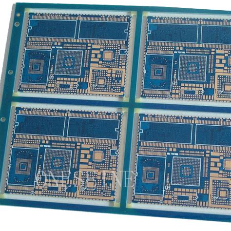
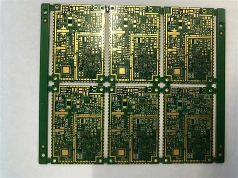
When tackling intricate electronics projects, selecting a 16 layer PCB manufacturer becomes critical for balancing performance, durability, and space optimization. High-layer-count boards demand precision in PCB manufacturing to manage signal integrity, thermal management, and interference reduction—factors that generic suppliers often overlook. Specialized PCB manufacturing companies leverage advanced techniques like laser drilling and sequential lamination to ensure layer alignment within microns, a necessity for high-speed or RF applications.
Complex designs often involve tight tolerances and dense component placement, which can escalate PCB manufacturing cost if not handled strategically. Experienced manufacturers optimize material selection and panel utilization to reduce waste, while maintaining IPC Class 3 standards for reliability. This expertise becomes vital when scaling prototypes to production, as inconsistencies in multilayer fabrication risk costly redesigns or field failures.
For businesses operating in the PCB manufacturing business, partnering with a certified 16-layer specialist mitigates risks associated with high-density interconnects (HDIs). These providers integrate design-for-manufacturability (DFM) checks early in the process, identifying potential issues like impedance mismatches or via stubs before they impact timelines. They also streamline assembly compatibility, ensuring seamless transitions from fabrication to component mounting—a key advantage for industries like aerospace or medical devices where reliability is non-negotiable.
Cost-Effective 16 Layer PCB Manufacturing Solutions
When sourcing 16-layer PCB manufacturing solutions, balancing pcb manufacturing cost with performance is critical. Leading pcb manufacturing companies achieve affordability through economies of scale, advanced fabrication processes, and strategic material sourcing. By optimizing layer stack-up designs and leveraging automated optical inspection (AOI) systems, they minimize waste while maintaining precision in high-density interconnects.
Your project’s pcb manufacturing business case benefits from suppliers that offer tiered pricing models, allowing you to scale production without compromising quality. For instance, streamlined DFM (Design for Manufacturing) checks reduce rework costs, while bulk material procurement lowers per-unit expenses. Modern manufacturers also employ hybrid HDI (High-Density Interconnect) techniques to reduce layer counts in complex layouts, further trimming pcb manufacturing overhead.
When evaluating costs, consider the total ownership value—reliable suppliers mitigate risks like signal integrity issues or thermal mismanagement, which can inflate long-term expenses. Transparent pricing structures ensure no hidden fees for impedance control or via filling, aligning with your budgetary needs. By partnering with specialized pcb manufacturing companies, you secure cost predictability without sacrificing the technical rigor required for 16-layer applications.
Advanced Multilayer PCB Fabrication Process Breakdown
Understanding the PCB manufacturing process for 16-layer boards begins with precision material selection. High-performance substrates like FR-4 or polyimide ensure thermal stability, while precision alignment during layer stacking minimizes signal loss. Leading PCB manufacturing companies employ laser drilling to create microvias as small as 0.1mm, enabling high-density interconnects critical for complex designs.
The lamination phase involves alternating copper and dielectric layers under extreme heat and pressure, a step where even minor deviations can compromise signal integrity. Automated optical inspection (AOI) systems then verify alignment accuracy, reducing defects before electroplating strengthens conductive pathways. Advanced PCB manufacturing business practices integrate impedance control testing here to guarantee performance in high-frequency applications.
Cost drivers in PCB manufacturing cost for multilayer builds include material waste reduction and yield optimization. Fabricators leverage direct imaging (DI) systems to minimize photoresist errors, while sequential lamination cycles ensure layer bonding without delamination risks. Finally, thermal management features like embedded copper coins or thermal vias are added to dissipate heat in high-power designs. By balancing these steps, trusted manufacturers deliver reliability without inflating project budgets.
Ensuring Reliability in 16-Layer PCB Production
Reliability in PCB manufacturing begins with precision at every stage, especially for complex 16-layer designs. To maintain signal integrity and thermal stability, manufacturers must implement stringent quality controls, from material selection to final testing. High-performance substrates, laser-drilled microvias, and advanced lamination techniques ensure consistent layer alignment and minimal impedance fluctuations—critical for high-speed or high-frequency applications.
When selecting PCB manufacturing companies, verify their certifications (e.g., ISO 9001, IPC Class 3) and inspect their process documentation. Reputable providers use automated optical inspection (AOI) and X-ray testing to detect hidden defects like voids or misregistration. For projects where PCB manufacturing cost is a priority, balancing material choices (e.g., FR-4 vs. high-Tg laminates) with performance requirements becomes essential without compromising reliability.
In the PCB manufacturing business, traceability systems are vital. Batch-level tracking of materials and production parameters allows quick root-cause analysis if issues arise post-deployment. Experienced manufacturers also conduct thermal cycling tests and accelerated life testing to simulate real-world operating conditions, ensuring boards withstand mechanical stress and environmental factors. By integrating these practices, you secure end products that align with both design specifications and long-term operational demands.
16 Layer PCB Assembly and Fabrication Synergy
When designing 16-layer PCBs, the seamless integration of assembly and fabrication processes becomes critical. Leading PCB manufacturing companies prioritize this synergy to eliminate bottlenecks, reduce PCB manufacturing cost, and ensure design intent translates flawlessly into functional boards. By aligning fabrication capabilities—such as laser-drilled microvias or controlled impedance layers—with assembly requirements like component placement density, you avoid costly redesigns and delays.
Advanced PCB manufacturing workflows employ cross-functional collaboration between design engineers and production teams. This ensures materials (e.g., high-Tg FR-4 or high-speed laminates) align with thermal and signal integrity needs during assembly. For instance, optimized layer stackups minimize crosstalk in high-density designs, while sequential lamination cycles preserve pad integrity for fine-pitch BGAs.
Moreover, unified quality control across fabrication and assembly stages—such as automated optical inspection (AOI) and X-ray testing—strengthens reliability. Trusted partners in the PCB manufacturing business leverage this integrated approach to balance performance with affordability, whether prototyping or scaling to volume production. By selecting a manufacturer that harmonizes these processes, you secure end-to-end solutions for even the most complex multilayer applications.
Trusted Partner for High-Density 16 Layer PCBs
When navigating the complexities of high-density 16-layer PCB manufacturing, partnering with experienced PCB manufacturing companies ensures your designs meet rigorous performance standards. These boards demand precision in layer alignment, signal integrity, and thermal management—areas where expertise directly impacts reliability. Reputable manufacturers leverage advanced processes like laser drilling and sequential lamination to achieve tight tolerances, critical for applications in aerospace, medical devices, or high-speed computing.
A key advantage lies in balancing PCB manufacturing cost with quality. Established providers optimize material selection and panel utilization, reducing waste while maintaining traceability across every production stage. This becomes vital when scaling your PCB manufacturing business, as consistent output minimizes delays and rework. Moreover, integrated testing protocols—such as automated optical inspection (AOI) and impedance control—ensure compliance with industry specifications, safeguarding your end products.
By aligning with a partner well-versed in PCB manufacturing for multilayer designs, you gain access to end-to-end solutions that streamline prototyping to mass production. Their technical support helps address challenges like via-in-pad configurations or mixed-signal layouts, ensuring your high-density boards perform flawlessly under demanding conditions.
Premium 16 Layer PCBs: Quality Meets Affordability
When sourcing 16-layer PCBs, balancing performance requirements with pcb manufacturing cost is critical. Leading pcb manufacturing companies achieve this equilibrium by optimizing material selection, leveraging advanced fabrication techniques, and streamlining production workflows. High-density designs demand precision, but that doesn’t equate to prohibitive expenses. Modern manufacturers employ economies of scale and automated processes to reduce waste, ensuring your pcb manufacturing business benefits from consistent quality without overspending.
Advanced stack-up configurations and controlled impedance management enable these multilayer boards to handle complex signal integrity needs while maintaining structural reliability. By partnering with a manufacturer that integrates pcb manufacturing and assembly under one roof, you eliminate logistical bottlenecks and reduce turnaround times. This synergy is particularly valuable for prototypes or mid-volume runs, where minimizing pcb manufacturing cost per unit directly impacts project viability.
Quality assurance protocols, such as automated optical inspection (AOI) and cross-sectional testing, ensure every layer meets IPC Class 3 standards. Transparent pricing models further align with budget constraints, allowing you to scale production efficiently. Whether you’re developing aerospace systems or medical devices, affordable 16-layer PCBs don’t require compromising on performance—they demand a partner who understands how to harmonize technical rigor with cost optimization.
Conclusion
When selecting a PCB manufacturing partner for intricate 16-layer designs, prioritizing technical expertise and proven reliability ensures your project’s success. Trusted PCB manufacturing companies leverage advanced fabrication techniques to balance performance with PCB manufacturing cost, delivering high-density boards that meet stringent quality benchmarks. Whether you’re scaling a PCB manufacturing business or developing mission-critical electronics, the synergy between multilayer fabrication and precision assembly becomes paramount for maintaining signal integrity and thermal stability.
By partnering with specialists who understand the complexities of 16-layer stack-ups, you gain access to optimized material selection, controlled impedance routing, and rigorous testing protocols—all critical for minimizing defects and ensuring long-term reliability. Moreover, transparent PCB manufacturing cost structures and scalable production workflows help avoid budget overruns without compromising on layer alignment or via-in-pad precision.
Ultimately, the right manufacturer acts as an extension of your engineering team, providing tailored solutions that align with your design goals. Look for partners who prioritize collaboration, offer end-to-end traceability, and maintain certifications for industries like aerospace or medical devices. This approach not only streamlines production but also future-proofs your electronics against evolving technical demands.
Frequently Asked Questions
What factors influence pcb manufacturing cost for 16-layer designs?
The complexity of multilayer stacking, material selection, and precision requirements for high-density interconnects (HDIs) directly affect pcb manufacturing cost. Advanced processes like laser drilling and impedance control add value but require specialized expertise from pcb manufacturing companies.
How do you ensure reliability in 16-layer PCBs?
Trusted pcb manufacturing partners use automated optical inspection (AOI), thermal stress testing, and signal integrity analysis. Rigorous quality checks at every production stage minimize defects, critical for high-performance applications.
Can a single provider handle both fabrication and assembly?
Yes. Leading pcb manufacturing business models integrate fabrication and assembly workflows. This synergy reduces lead times and ensures compatibility between multilayer boards and components, avoiding mismatches in tolerances or material properties.
Why choose specialized manufacturers for high-density designs?
Standard pcb manufacturing companies may lack the equipment or expertise for 16-layer boards. Specialized providers optimize processes like sequential lamination and via filling, ensuring signal integrity in compact, high-speed circuits.
How do you balance quality and affordability?
By leveraging economies of scale and process automation, competitive pcb manufacturing firms reduce waste while maintaining premium standards. Bulk ordering and design-for-manufacturability (DFM) consultations further optimize cost-efficiency.
Explore Custom 16-Layer PCB Solutions
For tailored guidance on complex multilayer designs, please click here to consult our engineering team at https://www.andwinpcb.com/pcb-manufacturing/.