Layer PCB Prototype Stackup and Testing Essentials
Key Takeaways
When designing 6-layer PCB prototypes, understanding core principles ensures success. Start by prioritizing signal integrity through optimized stackup configurations—typically arranging power, ground, and signal layers to minimize crosstalk. For example, a common stackup might pair high-speed signals between ground planes to reduce noise.
"Balancing thermal performance and electrical stability is non-negotiable in multilayer PCBs. Always validate your stackup with simulation tools before prototyping."
Next, address thermal management by selecting materials with high thermal conductivity (e.g., FR-4 with copper cores) and strategically placing vias for heat dissipation. Pair this with 4-wire testing protocols to verify trace resistance and detect microfractures early.
| Factor | Consideration | Impact on Cost |
|---|---|---|
| Material Selection | High-Tg FR-4 vs. Rogers | +15–30% |
| Layer Count | 6-layer vs. 4-layer | +20–40% |
| Testing Complexity | 4-wire vs. Basic Continuity | +10–25% |
For rapid 48-hour prototyping, collaborate with PCB manufacturing companies that automate CAM processes. While PCB manufacturing costs vary, bulk orders or standardized designs often reduce pricing to $2 per square inch. To cut expenses further, avoid over-engineering features like blind vias unless necessary.
Finally, consider via-in-pad technology for dense layouts, but verify compatibility with your PCB manufacturing business partner’s capabilities. Always request a Design for Manufacturability (DFM) review to preempt delays.
By aligning your design with these takeaways, you’ll streamline production while meeting performance benchmarks.
-Layer PCB Prototype Design Fundamentals
When designing a 6-layer PCB prototype, understanding stackup configuration is critical for balancing performance and pcb manufacturing cost. A typical stackup includes signal, power, and ground layers arranged to minimize electromagnetic interference (EMI) and crosstalk. Proper material selection—such as low-loss dielectrics or high-Tg laminates—directly impacts signal integrity and thermal stability, factors that pcb manufacturing companies prioritize to ensure reliability.
Your layer arrangement should account for controlled impedance routing, especially for high-speed signals. For instance, placing sensitive traces between ground planes reduces noise while optimizing power distribution. This approach not only enhances functionality but also streamlines production, reducing rework costs in the pcb manufacturing business.
Collaborate with fabricators early to align design choices with their capabilities. Advanced tools like impedance calculators and simulation software help validate stackup designs before prototyping. By integrating design-for-manufacturing (https://www.andwinpcba.com) that outline best practices for multilayer boards.
Balancing performance and cost requires iterative refinement. Test different configurations through simulation and consult technical specifications from your chosen pcb manufacturing partner to ensure feasibility. This proactive approach minimizes delays and aligns with rapid prototyping timelines while maintaining budget constraints.
Optimizing Signal Integrity Through Stackup
When designing a 6-layer PCB prototype, your stackup configuration directly impacts signal integrity and overall performance. Proper layer sequencing ensures minimal interference between high-speed signals, power planes, and ground layers. A typical optimal stackup might place signal layers adjacent to ground planes, creating controlled impedance paths while shielding sensitive traces from noise. For instance, placing high-frequency signals on inner layers sandwiched between ground planes reduces crosstalk and electromagnetic interference (EMI).
PCB manufacturing companies often recommend symmetrical stackups to prevent warping during fabrication, which becomes critical as PCB manufacturing costs rise with material waste. Using prepreg materials with low dielectric loss (e.g., FR-4 or high-speed variants) further stabilizes signal propagation. Pairing this with precise trace width calculations ensures impedance matching—vital for high-speed designs like DDR4 or USB 3.2.
Transitioning from design to production, collaborating with a reliable PCB manufacturing business helps validate stackup choices through simulation tools. These partnerships enable you to balance performance with PCB manufacturing cost constraints, ensuring prototypes meet both technical and budgetary requirements. By prioritizing stackup optimization early, you mitigate risks in later stages, such as signal degradation or re-spins, saving time and resources in the prototyping phase.
Thermal Management in Multilayer PCBs
When designing a 6-layer PCB prototype, thermal management becomes a critical consideration due to increased power density and confined heat dissipation pathways. PCB manufacturing processes for multilayer boards require careful stackup configuration, including strategically placed copper layers and dielectric materials with high thermal conductivity. Proper implementation of thermal vias—plated holes connecting layers—helps distribute heat away from hotspots, preventing component degradation. Optimizing via placement ensures efficient thermal transfer without compromising signal integrity.
Material selection also plays a pivotal role; using substrates like FR-4 with enhanced thermal properties or polyimide for high-temperature applications improves heat resistance. However, these choices directly impact PCB manufacturing cost, as specialized materials often come at a premium. When collaborating with PCB manufacturing companies, specify your thermal requirements early to align material choices and via designs with performance goals. Advanced simulation tools can predict thermal behavior during the design phase, reducing prototyping iterations. For instance, ensuring a glass transition temperature (Tg) above 170°C in the dielectric material prevents delamination under thermal stress.
This balance between thermal efficiency and PCB manufacturing business constraints requires evaluating trade-offs—such as opting for partial via-in-pad configurations instead of full copper fills to manage expenses. By prioritizing thermal management in your stackup design and material selection, you ensure reliable operation while maintaining cost-effectiveness—a necessity for high-density 6-layer prototypes in demanding applications.
4-Wire Testing Protocols for Quality Assurance
When verifying the electrical performance of PCB manufacturing outputs, 4-wire Kelvin testing provides unmatched precision for measuring low-resistance connections. Unlike traditional 2-wire methods, this protocol separates current injection and voltage measurement paths, eliminating lead resistance errors that could mask critical defects like micro-cracks or poor plating in vias. For PCB manufacturing companies, this approach ensures reliable data for impedance validation—especially vital in 6-layer designs where signal integrity depends on controlled trace resistance.
You’ll typically apply 4-wire testing to power planes, high-current traces, and via-in-pad structures. Advanced systems automate these measurements, aligning with rapid 48-hour turnaround demands while maintaining accuracy thresholds below ±1%. To optimize PCB manufacturing cost, engineers balance test coverage with cycle time, focusing on high-risk areas identified during stackup simulations. This targeted approach minimizes rework while meeting IPC-6012 standards for multilayer boards.
For PCB manufacturing business models prioritizing quality, integrating 4-wire protocols with thermal stress testing creates a robust quality assurance framework. Pairing these methods helps detect latent failures in materials or plating—key for avoiding field returns in applications demanding thermal management stability and long-term reliability.
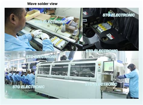
Rapid 48-Hour Prototyping Techniques
Achieving a 48-hour turnaround for PCB manufacturing requires streamlined workflows and advanced automation. Leading PCB manufacturing companies leverage high-speed drilling, laser direct imaging (LDI), and automated optical inspection (AOI) to reduce manual intervention. When implementing rapid prototyping, you’ll need to prioritize design files with clear layer stackup annotations to avoid delays during fabrication.
To maintain speed without compromising quality, design validation software is critical. These tools pre-check impedance mismatches and thermal hotspots, ensuring your 6-layer stackup aligns with signal integrity and thermal management requirements. For cost-sensitive projects, optimizing PCB manufacturing cost involves balancing material choices—such as mid-Tg FR-4 for reliability—and panel utilization rates.
Additionally, integrating 4-wire Kelvin testing during prototyping helps identify defects early, reducing rework cycles. Partnering with manufacturers offering just-in-time material sourcing ensures components arrive synchronized with production schedules. This approach not only accelerates timelines but also supports scalable PCB manufacturing business models.
Finally, verify if your supplier uses via-in-pad technology to minimize post-processing. By embedding vias directly into surface pads, you eliminate additional plating steps, shaving hours off the process. Such innovations enable 48-hour delivery while maintaining the precision demanded by high-density designs.
Cost-Effective PCB Manufacturing Solutions
When sourcing PCB manufacturing services, balancing quality and affordability requires strategic planning. Start by evaluating PCB manufacturing companies that specialize in multilayer designs, as their expertise in 6-layer PCB prototypes often translates to optimized processes and reduced waste. To minimize PCB manufacturing cost, consider design choices like standardized layer thicknesses or panelization strategies that maximize material utilization. Economies of scale play a role here—ordering larger prototype batches can lower per-unit expenses without compromising turnaround timelines.
Advanced PCB manufacturing business models now integrate automated workflows and predictive analytics to identify cost-saving opportunities early in the design phase. For instance, opting for FR-4 substrates instead of high-frequency materials for non-critical layers can trim expenses while maintaining performance. Additionally, partnering with manufacturers offering 48-hour prototyping ensures rapid iterations, reducing delays that inflate project budgets.
Always verify if suppliers provide transparent pricing tiers for testing and revisions. Some PCB manufacturing firms bundle services like 4-wire resistance testing into base packages, avoiding hidden fees. By aligning your design requirements with a manufacturer’s core capabilities, you achieve a cost structure that supports both prototyping agility and long-term scalability.
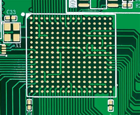
Via-in-Pad Technology Benefits Explained
When designing a 6-layer PCB prototype, via-in-pad technology addresses critical challenges in high-density layouts. By embedding vias directly into component pads, you eliminate the need for additional routing space, allowing tighter component placement and reduced board size. This is particularly valuable for PCB manufacturing companies working on compact devices, where every millimeter impacts functionality.
The technology enhances signal integrity by minimizing parasitic inductance and capacitance—common issues in traditional via placements. Shorter electrical paths between layers reduce signal reflection, which is crucial for high-speed circuits. Additionally, thermal vias integrated into pads improve heat dissipation, a key factor in thermal management for multilayer boards.
While PCB manufacturing cost may initially rise due to precise drilling and plating requirements, the long-term savings from improved yield and reduced rework justify the investment. For PCB manufacturing business models prioritizing reliability, via-in-pad reduces failure risks in demanding environments like automotive or IoT applications.
When partnering with PCB manufacturing providers, verify their capability to handle this technology. Advanced processes like laser drilling and filled vias ensure structural integrity, preventing solder wicking during assembly. By optimizing both performance and space efficiency, via-in-pad becomes a strategic choice for balancing complexity and cost-effectiveness in 6-layer prototypes.
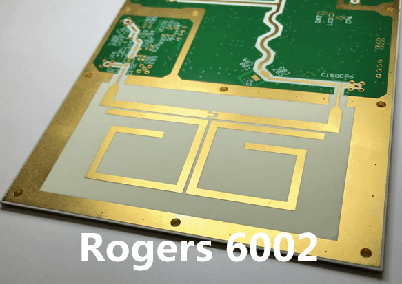
Choosing Materials for 6-Layer PCBs
When selecting materials for your 6-layer PCB prototype, prioritize thermal performance, signal integrity, and mechanical stability. High-frequency applications often require low-loss substrates like Rogers 4350B, while general-purpose designs may use FR-4 to minimize pcb manufacturing cost. For designs demanding superior thermal management, consider materials with enhanced thermal conductivity, such as Isola I-Tera MT40, to mitigate heat buildup in dense layouts.
PCB manufacturing companies typically offer material options tailored to your project’s electrical and environmental requirements. For instance, if your design involves via-in-pad technology, ensure the chosen substrate can withstand repeated thermal cycling during assembly. Balancing performance and cost is critical—premium materials may elevate pcb manufacturing business expenses but reduce long-term reliability risks.
Always verify dielectric constants (Dk) and dissipation factors (Df) with your manufacturer to avoid impedance mismatches. For pcb manufacturing workflows requiring rapid 48-hour turnaround, confirm material availability upfront to prevent delays. Finally, consult technical datasheets and leverage supplier expertise to align material choices with your prototype’s functional demands and budget constraints.
Conclusion
When finalizing your 6-layer PCB prototype, integrating stackup design with signal integrity and thermal management practices ensures reliable performance. By prioritizing PCB manufacturing partnerships with companies that adhere to rigorous 4-wire testing protocols, you validate quality while maintaining control over PCB manufacturing cost. Rapid 48-hour prototyping services enable iterative testing, crucial for refining designs before full-scale production.
Selecting materials that balance durability and thermal conductivity is key, especially when collaborating with PCB manufacturing companies specializing in high-density layouts. Via-in-pad technology further minimizes signal loss, aligning with advanced PCB manufacturing business standards. To optimize expenses, consider bulk prototyping or leveraging economies of scale without compromising on layer alignment accuracy.
Ultimately, a successful prototype hinges on aligning technical specifications with your project’s budget and timeline. Whether you’re addressing EMI challenges or fine-tuning power distribution, partnering with experienced PCB manufacturing providers ensures your design transitions seamlessly from prototype to mass production. This approach not only accelerates development cycles but also safeguards long-term reliability in demanding applications.
Frequently Asked Questions
How does stackup design impact signal integrity in 6-layer PCBs?
A well-optimized stackup minimizes electromagnetic interference and crosstalk by separating signal, power, and ground layers. Leading PCB manufacturing companies use simulations to validate impedance control, ensuring stable signal paths even in high-speed designs.
What thermal management techniques are recommended for multilayer boards?
Thermal vias and copper pours help dissipate heat, while selecting materials with low thermal resistance (e.g., FR-4 with high Tg) ensures reliability. Balancing these factors during PCB manufacturing prevents warping and extends board lifespan.
Why is 4-wire testing critical for quality assurance?
This method eliminates lead resistance errors, providing precise measurements for trace continuity and resistance. Rigorous testing protocols reduce defects, which is vital for maintaining competitiveness in the PCB manufacturing business.
How do manufacturers achieve 48-hour prototyping turnaround?
Automated processes, advanced CAM software, and streamlined workflows enable rapid production. Reputable PCB manufacturing companies prioritize material readiness and layer alignment checks to meet tight deadlines without compromising PCB manufacturing cost efficiency.
What factors influence PCB manufacturing cost for prototypes?
Layer count, material choice, surface finish, and testing requirements directly affect pricing. Optimizing designs for standard panel sizes and avoiding overly complex via structures can lower PCB manufacturing cost while maintaining performance.
Need a Reliable Partner for Your PCB Project?
For expert guidance on 6-layer prototypes, please click here to connect with AndwinPCB. Their team specializes in balancing performance, speed, and PCB manufacturing cost for demanding applications.