Layout and wiring issues that should be noted in PCB design when analog signals/digital signals are mixed
The operation of analog circuits depends on continuously changing currents and voltages. The operation of digital circuits depends on the detection of high or low levels at the receiving end according to pre-defined voltage levels or thresholds, which is equivalent to judging the “true” or “false” of the logic state.
There is a “gray” area between the high and low levels of digital circuits, in which digital circuits sometimes show analog effects. For example, when jumping from a low level to a high level (state), if the digital signal jumps fast enough, overshoot and ringback reflection will occur.
For modern board design, the concept of mixed-signal PCB is relatively vague, because even in purely “digital” devices, there are still analog circuits and analog effects. Therefore, in the early stages of design, in order to reliably achieve strict timing distribution, analog effects must be simulated. In fact, in addition to the reliability of communication products that must work continuously for several years without failure, the simulation of analog effects is particularly needed in mass-produced low-cost/high-performance consumer products.
Another difficulty in modern mixed-signal PCB design is that there are more and more devices with different digital logics, such as GTL, LVTTL, LVCMOS and LVDS logic.
The logic threshold and voltage swing of each logic circuit are different, but these circuits with different logic thresholds and voltage swings must be designed together on a PCB. Here, by thoroughly analyzing the layout and wiring design of high-density, high-performance, mixed-signal PCBs, you can master successful strategies and techniques.
Basics of Mixed-Signal Circuit Wiring
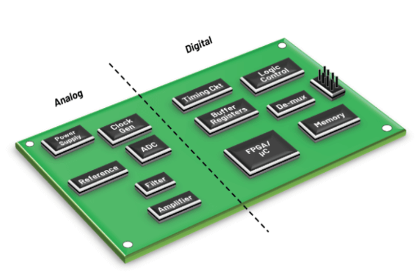
When digital and analog circuits share the same components on the same board, the layout and wiring of the circuit must be methodical. Only by revealing the characteristics of digital and analog circuits can the required PCB design goals be achieved in actual layout and wiring.
In mixed-signal PCB design, there are special requirements for power routing and the analog noise and digital circuit noise are required to be isolated from each other to avoid noise coupling, which increases the complexity of layout and wiring. The special needs for power transmission lines and the requirement to isolate noise coupling between analog and digital circuits further increase the complexity of mixed-signal PCB layout and routing.
If the power supply of the analog amplifier in the A/D converter is connected to the digital power supply of the A/D converter, it is very likely that the analog and digital circuits will affect each other. Perhaps, due to the location of the input/output connector, the layout scheme must mix the routing of digital and analog circuits.
Before layout and routing, engineers should understand the basic weaknesses of the layout and routing scheme. Even if there are false judgments, most engineers tend to use layout and routing information to identify potential electrical effects.
Layout and routing of modern mixed-signal PCBs
The following will explain the technology of mixed-signal PCB layout and routing through the design of OC48 interface cards. OC48 stands for Optical Carrier Standard 48, which is basically oriented to 2.5Gb serial optical communication. It is one of the high-capacity optical communication standards in modern communication equipment. The OC48 interface card contains several typical mixed-signal PCB layout and routing problems, and its layout and routing process will indicate the order and steps to solve the mixed-signal PCB layout scheme.
The OC48 card contains an optical transceiver that realizes bidirectional conversion between optical signals and analog electrical signals.
Analog signals are input or output to the digital signal processor, and the DSP converts these analog signals into digital logic levels, so that they can be connected to the microprocessor, programmable gate array, and the system interface circuits of the DSP and microprocessor on the OC48 card. Independent phase-locked loops, power supply filters, and local reference voltage sources are also integrated.
Among them, the microprocessor is a multi-power device with a main power supply of 2V and a 3.3V I/O signal power supply shared by other digital devices on the board. Independent digital clock sources provide clocks for OC48 I/O, microprocessors, and system I/O.
After checking the layout and wiring requirements of different functional circuit blocks, it is initially recommended to use a 12-layer board.
The configuration of microstrip and stripline layers can safely reduce the coupling of adjacent routing layers and improve impedance control. The ground layer is set between the first and second layers to isolate the wiring of sensitive analog reference sources, CPU cores, and PLL filter power supplies from the microprocessor and DSP devices on the first layer. Power and ground planes always appear in pairs, as is done on OC48 cards for shared 3.3V power planes. This will reduce the impedance between power and ground, thereby reducing noise on the power signal.
Avoid running digital clock lines and high-frequency analog signal lines near the power plane, otherwise the noise of the power signal will couple into sensitive analog signals.
Because 1-ounce copper clad laminates have strong ability to withstand high currents, 1-ounce copper clad laminates should be used for the 3.3V power plane and the corresponding ground plane, and 0.5-ounce copper clad laminates can be used for other layers, which can reduce voltage fluctuations caused by transient high currents or spikes.
If you design a complex system from the ground plane up, 0.093-inch and 0.100-inch thick cards should be used to support the wiring layer and the ground isolation layer. The thickness of the card must also be adjusted according to the wiring feature size of the via pad and the hole so that the aspect ratio of the drill hole diameter to the finished card thickness does not exceed the aspect ratio of the metallized hole provided by the manufacturer.
If you want to design a low-cost, high-volume commercial product with the minimum number of routing layers, carefully consider the routing details of all special power supplies on a mixed-signal PCB before layout or routing. Before starting layout and routing, have the target manufacturer review the preliminary layering plan. Basically, the layering should be based on the thickness of the finished product, the number of layers, the copper weight, the impedance (with tolerance), and the minimum via pad and hole size. The manufacturer should provide written layering recommendations.
The recommendations should include configuration examples for all controlled impedance stripline and microstrip lines. Combine your impedance predictions with the manufacturer’s impedance, and then use these impedance predictions to verify the signal routing characteristics in the simulation tools used to develop CAD routing rules.
OC48 card layout
The high-speed analog signals between the optical transceiver and the DSP are very sensitive to external noise. Similarly, all special power and reference voltage circuits also cause a lot of coupling between the analog and digital power transmission circuits of the card. Sometimes, due to the limitations of the chassis shape, you have to design a high-density board. Due to the orientation of the external optical cable access card and the high size of the optical transceiver component, the position of the transceiver in the card is largely fixed. The system I/O connector position and signal distribution are also fixed. This is the basic work that must be completed before layout.
Like most successful high-density analog layout and routing solutions, the layout must meet the routing requirements, and the layout and routing requirements must be balanced. For the analog part of a mixed-signal PCB and the local CPU core with a 2V operating voltage, the “layout first, then routing” method is not recommended. For the OC48 card, the DSP analog circuit part including the analog reference voltage and analog power bypass capacitor should be interactively routed first. After the routing is completed, the entire DSP with analog components and routing should be placed close enough to the optical transceiver to fully ensure the shortest routing length, minimum bends and vias from the high-speed analog differential signal to the DSP. The symmetry of the differential layout and routing will reduce the impact of common-mode noise. However, it is difficult to predict the best layout solution before routing.
Consult the chip distributor for the design guidelines for PCB layout.
Before designing according to the guidelines, fully communicate with the distributor’s application engineers. Many chip distributors have strict time limits for providing high-quality layout recommendations. Sometimes, the solutions they provide are feasible for the “first-tier customers” using the device. In the field of signal integrity (SI) design, signal integrity design for new devices is particularly important. According to the distributor’s basic guidelines and combined with the specific requirements of each power and ground pin in the package, you can start to layout and route the OC48 card integrating DSP and microprocessor.
After the location and routing of the high-frequency analog part are determined, the remaining digital circuits can be placed. Pay attention to the careful design of the following circuits: the location of the PLL power supply filtering circuit in the CPU with high sensitivity to analog signals; the local CPU core voltage regulator; the reference voltage circuit for the “digital” microprocessor.
The electrical and manufacturing guidelines for digital wiring can now be properly applied to the design.
The above-mentioned design of signal integrity for high-speed digital buses and clock signals reveals some special wiring topology requirements for processor buses, balanced Ts and skew matching of certain clock signal routing. But you may not know that some newer suggestions have been made, that is, adding several termination resistors.
In the process of solving problems, it is natural to make some adjustments at the layout stage. However, before starting the routing, it is important to verify the timing of the digital portion according to the layout scheme. At this point, a complete DFM/DFT layout review of the board will help ensure that the card meets the customer’s needs.
Digital Routing of OC48 Cards
For digital device power lines and the digital portion of mixed-signal DSPs, digital routing starts with SMD escape patterns. Use the shortest and widest traces allowed by the assembly process. For high-frequency devices, the power traces are equivalent to small inductors, which will worsen power supply noise and cause undesirable coupling between analog and digital circuits. The longer the power traces, the greater the inductance.
The best layout and routing scheme can be obtained by using digital bypass capacitors.
In short, fine-tune the location of the bypass capacitors as needed to make them easy to install and distributed around the digital components and the digital portion of the mixed-signal device. Use the same “shortest and widest routing” method to route the bypass capacitor escape patterns.
When power branches are to pass through a continuous plane (such as the 3.3V power
layer on an OC48 interface card), the power pins and bypass capacitors themselves do not have to share the same exit diagram to obtain the lowest inductance and ESR bypass. On mixed-signal PCBs such as OC48 interface cards, special attention should be paid to the routing of power branches. Remember to place additional bypass capacitors in a matrix arrangement across the entire card, even near passive devices.
After the power exit diagram is determined, automatic routing can begin.
ATE test contacts on OC48 cards are defined during logic design. Make sure that ATE contacts 100% of the nodes. In order to implement ATE testing with the minimum 0.070-inch ATE test probe, the location of the breakout via must be retained to ensure that the power layer is not interrupted by the antipads of the via.
If a power and ground layer split scheme is to be used, the offset layer (layer bias) should be selected on the adjacent routing layer parallel to the split. Define a no-route zone on the adjacent layer according to the perimeter of the opening area to prevent routing from entering. If routing must pass through the opening area to another layer, ensure that the other layer adjacent to the routing is a continuous ground layer. This will reduce the reflection path. Letting bypass capacitors cross the open power layer is beneficial for some digital signal layouts, but it is not recommended to bridge between digital and analog power layers because noise will couple each other through bypass capacitors.
Several new automatic routing applications can route high-density multi-layer digital circuits. In the initial routing stage, use a large 0.050-inch via spacing in the SMD export and consider the type of package used. The subsequent routing stage allows the vias to be located closer to each other, so that all tools can achieve the highest routing rate and the lowest number of vias. Because the OC48 processor bus uses a modified star topology, it has the highest priority in automatic routing.
Summary
After the OC48 card layout is completed, signal integrity verification and timing simulation should be performed. The simulation proves that the routing guidance meets the expected requirements and improves the timing indicators of the second-layer bus. Finally, the design rule check, final manufacturing review, mask and review are carried out and issued to the manufacturer, and the board layout task is officially completed.


