layout pcb online
Top Tools For Designing PCB Layouts Online
Designing printed circuit board (PCB) layouts has become increasingly accessible with the advent of online tools. These platforms offer a range of features that cater to both novice and experienced designers, streamlining the process and enhancing productivity. Among the top tools for designing PCB layouts online, several stand out due to their comprehensive capabilities, user-friendly interfaces, and robust support systems.
One of the most prominent tools in this domain is EasyEDA.
This platform is renowned for its intuitive interface and extensive library of components, which simplifies the design process. EasyEDA supports schematic capture, PCB layout, and even simulation, making it a versatile choice for various design needs. Additionally, its cloud-based nature allows for seamless collaboration among team members, ensuring that projects can be shared and edited in real-time. This feature is particularly beneficial for teams working remotely or across different geographical locations.
Transitioning to another notable tool, KiCad is an open-source software suite that has gained significant traction among PCB designers.
While it is not exclusively an online tool, its extensive online community and resources make it a valuable asset. KiCad offers a comprehensive set of features, including schematic capture, PCB layout, and 3D visualization. Its open-source nature means that users can customize the software to meet their specific needs, and the active community provides a wealth of tutorials, plugins, and support.
Another tool worth mentioning is Altium 365, which brings the power of Altium Designer to the cloud.
Altium 365 offers a collaborative environment where designers can work on PCB layouts, share designs, and manage projects efficiently. The platform integrates seamlessly with Altium Designer, providing a robust set of tools for schematic capture, PCB layout, and design rule checking. Moreover, Altium 365’s cloud-based infrastructure ensures that designs are securely stored and accessible from anywhere, facilitating collaboration and reducing the risk of data loss.
In addition to these tools, Autodesk’s Eagle is a well-established name in the PCB design industry.
Eagle’s online capabilities have been enhanced through its integration with Autodesk’s Fusion 360, providing a comprehensive solution for electronic and mechanical design. Eagle offers a user-friendly interface, extensive component libraries, and powerful design rule checking features. Its integration with Fusion 360 allows for seamless collaboration between electronic and mechanical engineers, ensuring that PCB designs are optimized for their intended applications.
Furthermore, Upverter is an innovative online tool that caters to both beginners and experienced designers.
Upverter’s browser-based platform offers a range of features, including schematic capture, PCB layout, and real-time collaboration. Its intuitive interface and extensive component library make it easy for users to get started, while its advanced features provide the flexibility needed for complex designs. Upverter’s collaborative capabilities are particularly noteworthy, allowing multiple users to work on a design simultaneously and see changes in real-time.
In conclusion, the landscape of PCB design has been significantly transformed by the availability of online tools. EasyEDA, KiCad, Altium 365, Eagle, and Upverter are among the top tools that offer a range of features to meet the diverse needs of PCB designers. These platforms not only simplify the design process but also enhance collaboration and productivity, making them invaluable assets in the field of electronic design. As technology continues to evolve, it is likely that these tools will become even more sophisticated, further streamlining the PCB design process and enabling designers to bring their ideas to life with greater efficiency and precision.
Step-By-Step Guide To Creating Your First Online PCB Layout
Creating your first online PCB layout can be an exciting yet challenging endeavor. The process involves several steps, each requiring careful attention to detail to ensure the final product meets your specifications. To begin with, it is essential to understand the basic components and tools required for PCB design. These include a computer with internet access, PCB design software, and a clear understanding of the circuit you intend to create.
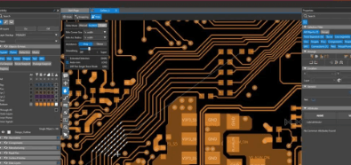
Initially, you must select an appropriate online PCB design tool.
Numerous options are available, each offering unique features and capabilities. Popular choices include EasyEDA, KiCad, and Altium Designer. These platforms provide user-friendly interfaces and extensive libraries of components, making them suitable for both beginners and experienced designers. Once you have chosen your design tool, the next step is to create a new project. This typically involves specifying the project name, dimensions of the PCB, and other relevant parameters.
Following the project setup, you will need to create a schematic diagram.
This diagram serves as a blueprint for your PCB layout, detailing the connections between various components. To do this, you will use the schematic editor within your chosen design tool. Begin by placing the components on the schematic canvas, ensuring each part is correctly labeled and oriented. Next, draw the connections, or nets, between the components, representing the electrical pathways. It is crucial to double-check these connections for accuracy, as errors at this stage can lead to significant issues later in the design process.
Once the schematic is complete, the next step is to convert it into a PCB layout.
This involves transferring the schematic components and connections onto a physical board layout. Most design tools offer an auto-router feature, which automatically generates the optimal routing for your PCB. However, manual adjustments may be necessary to fine-tune the layout and ensure all components fit within the specified dimensions. Pay close attention to the placement of components, as well as the routing of traces, to minimize potential issues such as signal interference or excessive heat generation.
After finalizing the PCB layout, it is essential to perform a design rule check (DRC).
This automated process verifies that your design adheres to the specified rules and constraints, such as minimum trace width and clearance. Any errors or violations identified during the DRC must be addressed before proceeding. Additionally, it is advisable to conduct a thorough visual inspection of the layout to identify any potential issues that may have been overlooked.
With the design verified, the next step is to generate the necessary files for manufacturing.
These typically include Gerber files, which contain the information required to produce the PCB, as well as a bill of materials (BOM) listing all components used in the design. Most online PCB design tools offer built-in functionality to generate these files, ensuring they are correctly formatted and ready for submission to a PCB manufacturer.
Finally, you will need to select a PCB manufacturer and submit your design files for production.
Many online services offer quick turnaround times and competitive pricing, making it easy to obtain high-quality PCBs. Once your order is placed, the manufacturer will produce and ship your PCBs, allowing you to assemble and test your completed circuit.
In conclusion, creating your first online PCB layout involves several critical steps, from selecting a design tool and creating a schematic to finalizing the layout and submitting your design for manufacturing. By following this step-by-step guide and paying close attention to detail, you can successfully navigate the process and bring your electronic projects to life.
Common Mistakes To Avoid In Online PCB Layout Design
Designing printed circuit boards (PCBs) online has become increasingly accessible, thanks to the proliferation of sophisticated software tools. However, despite the convenience and advanced features these tools offer, there are common mistakes that designers, especially novices, often make. Avoiding these pitfalls is crucial for ensuring the functionality, reliability, and manufacturability of the final product.
One of the most frequent errors in online PCB layout design is inadequate planning.
Many designers jump straight into the layout phase without a comprehensive schematic or a clear understanding of the circuit’s requirements. This lack of foresight can lead to inefficient layouts, signal integrity issues, and even complete circuit failure. Therefore, it is essential to start with a detailed schematic and a well-thought-out plan that considers all aspects of the design, including component placement, routing, and power distribution.
Another common mistake is improper component placement.
Components should be placed logically and strategically to minimize signal path lengths and avoid interference. Placing components haphazardly can result in complex routing, increased electromagnetic interference (EMI), and difficulties in troubleshooting. To mitigate this, designers should group related components together and place them in a manner that facilitates straightforward and efficient routing.
In addition to component placement, signal routing is another area where mistakes frequently occur.
Poor routing can lead to signal integrity problems, such as crosstalk, reflections, and noise. To avoid these issues, designers should follow best practices for routing, such as maintaining consistent trace widths, using proper grounding techniques, and avoiding sharp angles. Additionally, it is advisable to use differential pairs for high-speed signals and to keep signal traces as short as possible.
Thermal management is another critical aspect that is often overlooked in online PCB layout design.
Components generate heat, and if this heat is not properly managed, it can lead to component failure and reduced lifespan of the PCB. Designers should ensure adequate thermal relief by incorporating thermal vias, heat sinks, and proper spacing between components. Additionally, it is important to consider the thermal properties of the materials used in the PCB and to conduct thermal simulations to identify potential hotspots.
Furthermore, designers frequently neglect the importance of design for manufacturability (DFM).
A PCB layout that looks good on screen may not be feasible to manufacture. Issues such as insufficient trace clearances, inappropriate pad sizes, and non-standard component footprints can lead to manufacturing defects and increased production costs. To avoid these problems, designers should adhere to the design rules provided by the PCB manufacturer and use DFM tools to validate their designs before finalizing them.
Lastly, inadequate documentation is a common mistake that can cause significant issues during the manufacturing and assembly process.
Comprehensive documentation, including detailed schematics, bill of materials (BOM), and assembly drawings, is essential for ensuring that the PCB is manufactured and assembled correctly. Designers should take the time to create thorough and accurate documentation to avoid misunderstandings and errors.
In conclusion, while online PCB layout design tools offer tremendous convenience and capabilities, it is crucial to avoid common mistakes that can compromise the quality and functionality of the final product. By planning thoroughly, placing components strategically, routing signals carefully, managing thermal properties, considering manufacturability, and providing comprehensive documentation, designers can create reliable and efficient PCBs that meet their intended specifications.

Benefits Of Using Online Platforms For PCB Layout Design
The advent of online platforms for PCB layout design has revolutionized the electronics industry, offering numerous benefits that streamline the design process and enhance overall efficiency. One of the most significant advantages of using online platforms is the accessibility they provide. Engineers and designers can access these tools from anywhere in the world, eliminating the need for physical presence in a specific location. This flexibility is particularly beneficial in today’s globalized work environment, where teams are often dispersed across different regions.
Moreover, online PCB layout design platforms often come equipped with a wide array of features that simplify the design process.
These tools typically include extensive libraries of components, which can be easily integrated into the design. This not only saves time but also ensures that the components used are up-to-date and compliant with industry standards. Additionally, many online platforms offer real-time collaboration features, allowing multiple team members to work on the same project simultaneously. This collaborative approach fosters innovation and accelerates the design process, as team members can share ideas and feedback instantaneously.
Another notable benefit is the cost-effectiveness of using online platforms for PCB layout design.
Traditional design software often requires substantial upfront investment and ongoing maintenance costs. In contrast, many online platforms operate on a subscription basis, which can be more affordable for both small businesses and large enterprises. Furthermore, these platforms frequently offer scalable solutions, allowing users to choose a plan that best fits their needs and budget. This scalability ensures that companies only pay for the features they require, making the design process more economical.
In addition to cost savings, online PCB layout design platforms also enhance the accuracy and reliability of the designs.
Advanced simulation and validation tools are often integrated into these platforms, enabling designers to test their circuits before moving to the production phase. This preemptive testing helps identify potential issues early in the design process, reducing the risk of costly errors and rework. Consequently, the overall quality of the final product is improved, leading to higher customer satisfaction and reduced time-to-market.
Furthermore, the user-friendly interfaces of many online PCB layout design platforms make them accessible to both novice and experienced designers.
Intuitive drag-and-drop functionalities, along with comprehensive tutorials and support resources, ensure that users can quickly become proficient in using the tools. This ease of use not only shortens the learning curve but also empowers designers to focus more on creativity and innovation rather than grappling with complex software.
The integration capabilities of online platforms also play a crucial role in streamlining the design process.
Many of these platforms can seamlessly integrate with other software tools and systems, such as CAD programs and manufacturing services. This interoperability facilitates a smooth transition from design to production, ensuring that all aspects of the project are aligned and cohesive. As a result, the entire workflow becomes more efficient, reducing delays and enhancing productivity.
In conclusion, the benefits of using online platforms for PCB layout design are manifold. From enhanced accessibility and real-time collaboration to cost-effectiveness and improved accuracy, these platforms offer a comprehensive solution that meets the diverse needs of modern electronics design. By leveraging the advanced features and user-friendly interfaces of online tools, designers can achieve higher quality outcomes, faster turnaround times, and greater overall efficiency. As the electronics industry continues to evolve, the adoption of online PCB layout design platforms is poised to become an increasingly integral part of the design process.