Lightweight Printed Circuit Boards: Design, Materials, and Applications
Abstract
Lightweight printed circuit boards (PCBs) are becoming increasingly important in modern electronics, especially in aerospace, automotive, and portable consumer devices where weight reduction is critical. This article explores the key aspects of lightweight PCBs, including material selection, design optimization, manufacturing techniques, and applications. We discuss advanced materials such as flexible substrates, thin copper layers, and composite materials that contribute to weight reduction while maintaining performance. Additionally, we examine design strategies like high-density interconnects (HDI) and embedded components that help minimize PCB mass. Finally, we highlight industry trends and future developments in lightweight PCB technology.

1. Introduction
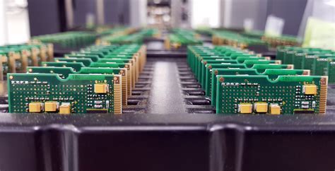
Printed circuit boards (PCBs) are essential components in nearly all electronic devices, providing mechanical support and electrical connections between components. As electronics become more compact and portable, the demand for lightweight PCBs has grown significantly. Industries such as aerospace, automotive, and wearable technology require PCBs that are not only functional but also as light as possible to improve efficiency, reduce energy consumption, and enhance portability.
Lightweight PCBs achieve mass reduction through innovative materials, optimized layouts, and advanced manufacturing techniques. This article provides a comprehensive overview of the technologies and
methodologies used to develop lightweight PCBs while ensuring reliability and performance.
2. Materials for Lightweight PCBs
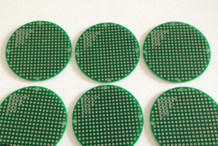
2.1 Thin Substrates
Traditional PCBs use FR-4, a glass-reinforced epoxy laminate, which provides good mechanical strength but adds weight. Lightweight alternatives include:
- Polyimide Films: Used in flexible PCBs, polyimide is lightweight and heat-resistant.
- Liquid Crystal Polymer (LCP): Offers excellent high-frequency performance with minimal weight.
- Thin-core FR-4: Reducing the thickness of standard FR-4 lowers weight while maintaining rigidity.
2.2 Lightweight Copper Layers
Copper traces contribute significantly to PCB weight. Strategies to reduce copper mass include:
- Thin Copper Foils: Using ½ oz (17.5 µm) or ⅓ oz (12 µm) copper instead of standard 1 oz (35 µm).
- Selective Copper Deposition: Applying copper only where needed reduces excess material.
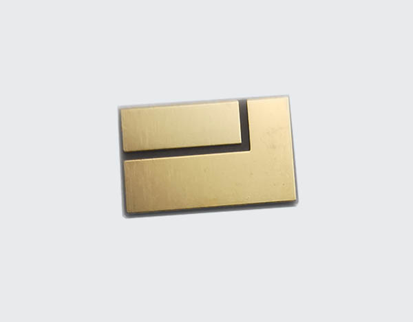
2.3 Advanced Composite Materials
- Metal-core PCBs with Aluminum or Magnesium: These provide structural support with lower weight than traditional materials.
- Carbon Fiber Reinforced Polymers (CFRP): Used in high-performance applications where strength-to-weight ratio is crucial.
3. Design Strategies for Lightweight PCBs
3.1 High-Density Interconnect (HDI) Technology
HDI PCBs use finer traces, microvias, and blind/buried vias to reduce layer count and overall weight. Benefits include:
- Fewer layers required for the same functionality.
- Reduced material usage without sacrificing performance.
3.2 Embedded Components
Embedding passive components (resistors, capacitors) within the PCB layers eliminates the need for surface-mounted devices (SMDs), reducing weight and improving space efficiency.
3.3 Optimized Layer Stackup
- Using asymmetric stackups where possible to minimize unnecessary layers.
- Combining signal and power layers efficiently to reduce thickness.
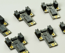
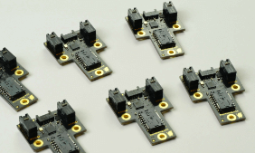
3.4 Flexible and Rigid-Flex PCBs
Flexible PCBs eliminate heavy connectors and rigid supports, making them ideal for weight-sensitive applications. Rigid-flex designs combine the benefits of both rigid and flexible PCBs, optimizing weight and durability.
4. Manufacturing Techniques for Lightweight PCBs
4.1 Laser Drilling and Microvia Technology
Laser drilling enables smaller vias, allowing for higher routing density and reduced layer count.
4.2 Additive Manufacturing (3D Printing)
3D-printed PCBs use conductive inks and lightweight polymers to create custom, low-mass circuit boards.
4.3 Selective Surface Finishing
Instead of applying finishes (e.g., ENIG, HASL) across the entire board, selective finishing reduces material usage.
5. Applications of Lightweight PCBs
5.1 Aerospace and UAVs
- Satellites, drones, and aircraft benefit from weight savings, improving fuel efficiency and payload capacity.
5.2 Automotive Electronics
- Electric vehicles (EVs) use lightweight PCBs to extend battery life and reduce overall vehicle weight.
5.3 Wearable and Medical Devices
- Smartwatches, fitness trackers, and implantable medical devices require ultra-light PCBs for comfort and functionality.
5.4 Consumer Electronics
- Smartphones, tablets, and laptops utilize lightweight PCBs to enhance portability.
6. Challenges and Future Trends
6.1 Thermal Management
Reducing material thickness can impact heat dissipation. Advanced thermal management techniques, such as embedded heat sinks, are being developed.
6.2 Signal Integrity
Thinner substrates and traces may affect high-speed signal performance. Innovations in dielectric materials help mitigate these issues.
6.3 Sustainability
Eco-friendly lightweight materials, such as biodegradable substrates, are emerging as a key trend.
6.4 Future Developments
- Graphene-based PCBs: Promising ultra-lightweight and high-conductivity properties.
- Self-healing Materials: Could enhance durability in lightweight PCBs.
7. Conclusion
Lightweight PCBs are a critical enabler for next-generation electronics, offering significant advantages in industries where weight reduction is paramount. Advances in materials, design methodologies, and manufacturing techniques continue to push the boundaries of what is possible. As technology evolves, lightweight PCBs will play an even greater role in aerospace, automotive, and portable electronics, driving innovation across multiple sectors.