Low-Loss PCB: Design, Materials, and Applications in High-Frequency Circuits
Introduction to Low-Loss PCBs
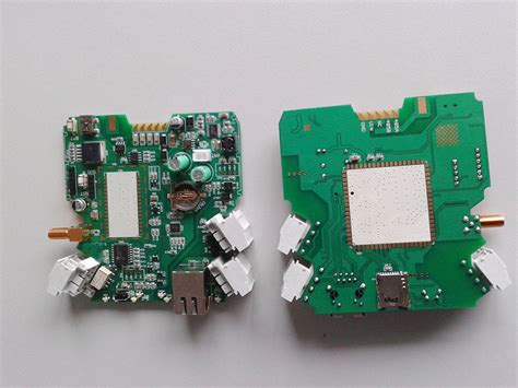
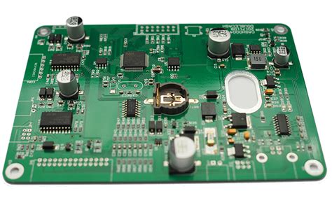
Printed Circuit Boards (PCBs) have become the backbone of modern electronics, and as signal frequencies continue to rise in applications ranging from 5G communications to advanced radar systems, the demand for low-loss PCBs has grown exponentially. Low-loss PCBs are specialized circuit boards designed to minimize signal attenuation, maintain signal integrity, and reduce energy dissipation at high frequencies.
Traditional FR-4 PCBs, while cost-effective for many applications, exhibit significant signal loss at frequencies above a few gigahertz. This limitation has driven the development of advanced low-loss materials and innovative PCB design techniques. Low-loss PCBs typically demonstrate a dissipation factor (Df) below 0.004 and a stable dielectric constant (Dk) across wide frequency ranges, enabling them to support high-frequency applications with minimal signal degradation.
The importance of low-loss PCBs extends across numerous industries. In telecommunications, they enable higher data rates and longer transmission distances. In aerospace and defense applications, they improve radar performance and reliability. For consumer electronics, they support the next generation of wireless devices with faster processing and improved energy efficiency.
Key Characteristics of Low-Loss PCB Materials
Dielectric Constant (Dk) and Its Stability
The dielectric constant, or relative permittivity (Dk), is a fundamental property of PCB materials that affects signal propagation speed and impedance. Low-loss materials typically have Dk values ranging from 2.5 to 3.5, compared to standard FR-4’s 4.3-4.8 at 1 GHz. More importantly, high-quality low-loss materials maintain consistent Dk across frequency ranges (up to 40 GHz or higher) and under varying environmental conditions.
Materials with stable Dk prevent impedance variations that can cause signal reflections and integrity issues. This stability becomes increasingly critical as signal rise times decrease in high-speed digital applications. Manufacturers achieve this stability through precise control of material composition and the use of fillers that minimize frequency-dependent effects.
Dissipation Factor (Df) and Loss Mechanisms
The dissipation factor (Df), also called loss tangent, quantifies a material’s inherent signal loss. While FR-4 typically has a Df of 0.02 at 1 GHz, advanced low-loss materials achieve Df values as low as 0.001. This order-of-magnitude improvement directly translates to significantly reduced dielectric losses.
Signal loss in PCBs occurs through several mechanisms:
- Dielectric loss: Energy absorbed by the substrate material
- Conductor loss: Resistance in copper traces, exacerbated by skin effect at high frequencies
- Radiation loss: Energy lost to electromagnetic radiation
- Surface wave loss: Energy coupled into substrate surface waves
Low-loss materials primarily address dielectric loss, but optimal PCB design must consider all loss mechanisms holistically.
Thermal Management Properties
High-frequency circuits often generate substantial heat, making thermal management crucial. Low-loss materials typically exhibit superior thermal conductivity (0.5-1.5 W/mK) compared to FR-4 (0.3 W/mK), allowing better heat dissipation. They also maintain stable electrical properties across temperature ranges (-50°C to +150°C for many high-end materials).
Coefficient of Thermal Expansion (CTE) matching is another critical factor. Materials with CTE closely matching copper (about 17 ppm/°C) reduce mechanical stress during temperature cycling, improving reliability. Many low-loss materials achieve this through sophisticated filler systems or reinforced structures.
Common Low-Loss PCB Materials
PTFE-Based Materials
Polytetrafluoroethylene (PTFE) substrates, often marketed under the Teflon brand, represent the gold standard for low-loss applications. Pure PTFE offers exceptional electrical properties (Dk ≈ 2.1, Df ≈ 0.0004) but presents manufacturing challenges due to its softness and high CTE. Modified PTFE composites address these issues:
- RT/duroid 5880: Dk 2.2 ± 0.02, Df 0.0009 (up to 10 GHz)
- Taconic TLY: Dk 2.2, Df 0.0009, with improved mechanical stability
- Rogers RO3000 series: PTFE with ceramic fillers, Dk 3.0, Df 0.0013
These materials excel in millimeter-wave applications but require specialized processing techniques for drilling, plating, and soldering.
Hydrocarbon-Based Ceramic Filled Materials
For applications balancing performance and cost, hydrocarbon resins with ceramic fillers provide excellent alternatives:
- Rogers RO4000 series: Dk 3.3-3.7, Df 0.0027-0.0037, compatible with FR-4 processes
- Isola I-Tera MT40: Dk 3.45, Df 0.0031, designed for lead-free assembly
- Nelco N4000-13: Dk 3.7, Df 0.008, with good thermal performance
These materials offer easier fabrication than PTFE while still providing substantial improvements over standard FR-4.
Liquid Crystal Polymer (LCP)
LCP has emerged as a compelling option for ultra-high-frequency applications (up to 110 GHz):
- Anisotropic properties allow tuning of Dk in different directions
- Naturally low moisture absorption (<0.1%)
- Thin-film capabilities suitable for flexible circuits
- Dk ≈ 3.0, Df ≈ 0.002-0.004 depending on formulation
LCP finds particular use in millimeter-wave applications and flexible high-frequency circuits.
Design Considerations for Low-Loss PCBs
Transmission Line Structures
Proper transmission line design is paramount for maintaining signal integrity:
- Microstrip: Common for surface layers, easy to fabricate but susceptible to radiation losses at high frequencies
- Stripline: Sandwiched between ground planes, minimizes radiation but increases fabrication complexity
- Coplanar Waveguide (CPW): Ground planes on the same layer as signal, excellent for high-frequency but sensitive to solder mask
- Grounded Coplanar Waveguide (GCPW): Combines CPW with bottom ground plane, offering best performance for many high-frequency designs
Impedance control becomes more challenging with low-Dk materials, as the same impedance requires wider traces or smaller dielectric spacing compared to FR-4.
Copper Surface Roughness
At high frequencies, current concentrates near conductor surfaces (skin effect). Standard copper foil roughness (typically 2-3 μm RMS) can significantly increase conductor losses. Strategies to mitigate this include:
- Using ultra-low-profile copper (≤1 μm RMS)
- Electrodeposited copper with additive grain refiners
- Rolled copper alternatives
- Surface treatments that reduce roughness without compromising adhesion
For extreme high-frequency applications (≥30 GHz), foil choices can affect insertion loss by 20% or more.
Via Design and Transition Optimization
Vertical interconnects often become weak points in high-frequency designs:
- Via stub effects: Can cause resonances; back-drilling or blind vias eliminate unused via portions
- Anti-pad sizing: Critical for maintaining impedance through layers
- Via fencing: Grounded vias around critical signals control mode conversion and radiation
- Via transition design: Tapered or stepped transitions minimize impedance discontinuities
Simulation tools (3D EM solvers) are essential for optimizing these structures before fabrication.
Manufacturing Challenges and Solutions
Material Handling and Processing
Low-loss materials often require specialized handling:
- PTFE materials need plasma treatment or sodium etch for proper copper adhesion
- Many high-frequency laminates are softer than FR-4, requiring adjusted drilling parameters
- Low-CTE materials may need modified lamination cycles to prevent warpage
- Some materials are sensitive to standard cleaning chemistries
Tight Tolerances and Registration
High-frequency designs demand tighter tolerances than conventional PCBs:
- Typical impedance tolerance requirements of ±5% or better
- Layer-to-layer registration often ≤25 μm
- Etch control critical for maintaining consistent line widths
- Thickness control of dielectric layers within ±5%
Advanced fabrication equipment (laser direct imaging, high-precision lamination) helps achieve these requirements.
Surface Finishes and Their Impact
Standard surface finishes can introduce unacceptable losses at high frequencies:
- Electroless Nickel Immersion Gold (ENIG): Nickel’s magnetic properties increase loss; thin nickel layers help
- Immersion Silver: Lower loss but susceptible to tarnishing
- Electrolytic Hard Gold: Good for RF but expensive and requires careful thickness control
- Organic Solderability Preservatives (OSP): Lowest loss but limited shelf life
- Immersion Tin: Moderate loss characteristics with good solderability
Finish selection must balance electrical performance, reliability, and assembly requirements.
Testing and Characterization Methods
Time-Domain Reflectometry (TDR)
TDR provides critical insights into impedance consistency and discontinuities:
- Measures impedance profile along transmission lines
- Identifies defects like necking, plating voids, or material inconsistencies
- Typical TDR systems offer resolutions down to 20-30 ps
Vector Network Analyzer (VNA) Measurements
VNA testing quantifies high-frequency performance:
- S-parameters (S11, S21 especially) characterize loss and reflections
- Frequency ranges up to 110 GHz for advanced systems
- Calibration standards critical for accurate measurements
- Fixture de-embedding removes test setup effects
Resonator Methods
For material property characterization:
- Split-post dielectric resonators measure Dk and Df with high accuracy
- Fabry-Perot resonators suitable for thin-film materials
- Cavity perturbation methods for small samples
Applications of Low-Loss PCBs
5G Infrastructure and Devices
- Millimeter-wave base station antennas (24-39 GHz bands)
- Massive MIMO array substrates
- Front-end modules with integrated antennas
- Low-loss requirements increase with frequency (e.g., 28 GHz vs. sub-6 GHz)
Aerospace and Defense Systems
- Phased array radar systems
- Electronic warfare platforms
- Satellite communications
- Avionics with combined RF/digital functionality
Automotive Radar
- 77-81 GHz autonomous vehicle sensors
- Compact radar modules with integrated processing
- Materials must withstand automotive environmental stresses
High-Speed Digital Applications
- Server backplanes for 112 Gbps PAM4 signaling
- Optical transceiver interfaces
- High-performance computing interconnects
- Loss budgets become critical as data rates exceed 25 Gbps per lane
Future Trends in Low-Loss PCB Technology
Heterogeneous Integration
Combining multiple material types within a single PCB:
- High-speed digital sections with moderate loss materials
- RF sections with ultra-low-loss materials
- Embedded passives and actives
- Advanced packaging techniques (2.5D, 3D integration)
Additive Manufacturing Approaches
- Inkjet-printed high-frequency circuits
- Aerosol jet for fine-feature deposition
- Potential for graded dielectric constant materials
Advanced Material Development
- Nanocomposite dielectrics with tailored properties
- Metamaterial approaches for unusual Dk/Df combinations
- Improved thermoset systems competing with PTFE performance
- Sustainable low-loss material options
Design Automation Tools
- AI-assisted layout optimization
- Faster 3D EM simulation techniques
- Integrated thermal-electrical-mechanical analysis
- Digital twin approaches for manufacturing correlation
Conclusion
Low-loss PCB technology sits at the crossroads of materials science, precision manufacturing, and advanced electrical design. As electronic systems push into higher frequency regimes and demand faster data rates, the importance of low-loss solutions will only grow. Successful implementation requires careful consideration of material properties, design techniques, and manufacturing processes—all working in concert to achieve optimal performance. The future promises even more sophisticated approaches as traditional scaling challenges meet innovative new technologies in this critical field of electronic engineering.