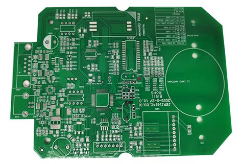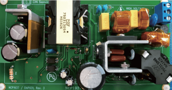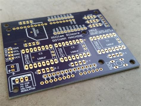
M-flex pcb
Advantages Of M-Flex PCB In Modern Electronics
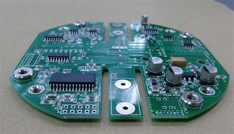
M-flex PCBs, or flexible printed circuit boards, have become a cornerstone in the evolution of modern electronics, offering a myriad of advantages that cater to the ever-growing demand for compact, efficient, and reliable electronic devices. As technology continues to advance, the need for components that can adapt to various shapes and spaces has become increasingly important. M-flex PCBs address this need by providing a versatile solution that traditional rigid PCBs cannot match.
One of the primary advantages of M-flex PCBs is their inherent flexibility, which allows them to be bent, folded, or twisted to fit into unconventional spaces.
This characteristic is particularly beneficial in the design of compact electronic devices, such as smartphones, wearable technology, and medical devices, where space is at a premium. By utilizing M-flex PCBs, manufacturers can create more ergonomic and aesthetically pleasing products without compromising on functionality or performance.
In addition to their flexibility, M-flex PCBs offer significant weight and space savings.
Traditional rigid PCBs often require additional connectors and cables to link different components, which can add bulk and weight to the final product. In contrast, M-flex PCBs can integrate multiple components onto a single board, reducing the need for extra connectors and cables. This not only results in a lighter and more compact device but also simplifies the assembly process, leading to reduced manufacturing costs and time.
Moreover, M-flex PCBs are known for their durability and reliability, which are crucial factors in the performance of modern electronic devices.
The materials used in the construction of M-flex PCBs are designed to withstand harsh environmental conditions, such as extreme temperatures, humidity, and vibrations. This makes them ideal for use in applications where reliability is paramount, such as in automotive, aerospace, and military industries. The ability of M-flex PCBs to maintain their performance under such conditions ensures that devices remain operational and efficient over extended periods.
Another notable advantage of M-flex PCBs is their potential for enhanced electrical performance.
The design flexibility of these boards allows for shorter signal paths, which can lead to reduced signal loss and improved electrical performance. This is particularly important in high-frequency applications, where maintaining signal integrity is critical. By minimizing the distance that signals must travel, M-flex PCBs can help reduce electromagnetic interference and improve overall device performance.
Furthermore, the use of M-flex PCBs can contribute to more sustainable manufacturing practices.
The reduction in materials and components required for assembly not only decreases waste but also lowers the energy consumption associated with production. As the electronics industry continues to prioritize sustainability, the adoption of M-flex PCBs represents a step towards more environmentally friendly manufacturing processes.
In conclusion, the advantages of M-flex PCBs in modern electronics are manifold, encompassing flexibility, weight and space savings, durability, enhanced electrical performance, and sustainability. As the demand for smaller, more efficient, and reliable electronic devices continues to grow, the role of M-flex PCBs in meeting these requirements becomes increasingly significant. By offering a versatile and adaptable solution, M-flex PCBs are poised to remain an integral component in the development of cutting-edge electronic technologies.
Design Considerations For M-Flex PCB Applications
When designing m-flex PCBs, or multilayer flexible printed circuit boards, several critical considerations must be taken into account to ensure optimal performance and reliability. These advanced circuit boards are increasingly utilized in a variety of applications due to their ability to conform to complex shapes and their lightweight nature. As such, understanding the nuances of their design is essential for engineers and designers aiming to leverage their full potential.
To begin with, material selection is a fundamental aspect of m-flex PCB design.
The choice of substrate material significantly influences the board’s flexibility, thermal stability, and overall durability. Polyimide is a popular choice due to its excellent thermal resistance and flexibility, making it suitable for applications that require bending and folding. However, the specific application requirements should guide the selection process, as different materials offer varying degrees of flexibility and thermal performance.
In addition to material selection, the layout of the circuit is another crucial consideration.
The design must accommodate the unique properties of flexible circuits, such as their ability to bend and twist. This requires careful planning of the trace layout to prevent stress concentration, which can lead to mechanical failure. Designers often employ techniques such as curved traces and staggered vias to distribute stress more evenly across the board. Moreover, the use of reinforcement materials, such as stiffeners, can provide additional support in areas that are subject to frequent bending.
Furthermore, the thickness of the m-flex PCB plays a significant role in its performance.
Thinner boards offer greater flexibility, which is advantageous in applications where space is limited or where the board must conform to intricate shapes. However, thinner boards may also be more susceptible to damage from mechanical stress. Therefore, striking a balance between flexibility and durability is essential. This balance can be achieved by optimizing the layer stack-up and selecting appropriate materials for each layer.
Thermal management is another critical aspect of m-flex PCB design.
Due to their compact nature, these boards can be prone to overheating, which can adversely affect their performance and longevity. Effective thermal management strategies, such as the incorporation of thermal vias and the use of heat-dissipating materials, are essential to mitigate this risk. Additionally, designers should consider the operating environment and ensure that the board can withstand the expected temperature range.
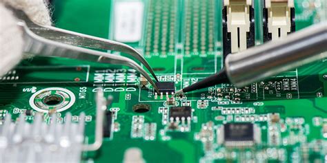
Moreover, the assembly process for m-flex PCBs requires special attention.
The flexible nature of these boards necessitates careful handling to prevent damage during assembly. Techniques such as controlled bending and the use of specialized fixtures can help maintain the integrity of the board during this process. Additionally, the choice of soldering method and the selection of appropriate adhesives are crucial to ensure reliable connections and to prevent delamination.
In conclusion, designing m-flex PCBs involves a comprehensive understanding of various factors, including material selection, circuit layout, board thickness, thermal management, and assembly processes. By carefully considering these elements, designers can create flexible circuit boards that meet the specific demands of their applications, ensuring both performance and reliability. As technology continues to advance, the importance of these considerations will only grow, making it imperative for designers to stay informed about the latest developments in m-flex PCB design.

Manufacturing Process Of M-Flex PCB: A Step-By-Step Guide
The manufacturing process of M-Flex PCBs, or multilayer flexible printed circuit boards, is a sophisticated procedure that requires precision and expertise. These PCBs are integral to modern electronics, offering flexibility and durability that traditional rigid PCBs cannot match. The process begins with the design phase, where engineers use specialized software to create a detailed blueprint of the circuit. This design is crucial as it dictates the layout and functionality of the final product. Once the design is finalized, it is transferred onto a flexible substrate, typically made of polyimide, which is known for its excellent thermal stability and flexibility.
Following the design transfer, the substrate undergoes a cleaning process to ensure that it is free from any contaminants that could affect the adhesion of the subsequent layers.
This step is critical as any impurities can lead to defects in the final product. After cleaning, a layer of copper is laminated onto the substrate. This copper layer serves as the conductive material for the circuit. The lamination process involves applying heat and pressure to bond the copper to the substrate, ensuring a strong and reliable connection.
Once the copper is laminated, the next step is to apply a photoresist layer.
This light-sensitive material is used to define the circuit pattern. The photoresist is exposed to ultraviolet light through a mask that contains the circuit design. The areas exposed to the light harden, while the unexposed areas remain soft and are subsequently washed away, revealing the copper pattern beneath. This process is known as photolithography and is a critical step in defining the intricate pathways of the circuit.
With the circuit pattern established, the next phase involves etching away the excess copper.
This is done using a chemical solution that removes the unwanted copper, leaving only the desired circuit pattern intact. The precision of this step is paramount, as any errors can lead to short circuits or open circuits in the final product. After etching, the remaining photoresist is stripped away, leaving a clean and precise copper circuit on the flexible substrate.
The process then moves to the drilling phase, where holes are created for vias and through-hole components.
These holes are drilled using precision machinery to ensure accuracy and alignment with the circuit design. Once drilled, the holes are plated with copper to establish electrical connections between the different layers of the PCB.
Following drilling and plating, the M-Flex PCB undergoes a series of inspections and tests to ensure its functionality and reliability.
These tests include electrical testing to verify the integrity of the circuit and visual inspections to check for any physical defects. Any issues identified during this phase are addressed before the PCB moves to the final stages of production.
The final steps in the manufacturing process involve applying a protective solder mask and screen printing the component labels onto the PCB. The solder mask protects the copper traces from oxidation and prevents solder bridges during component assembly. The screen printing provides clear identification of component placement, aiding in the assembly process.
In conclusion, the manufacturing process of M-Flex PCBs is a meticulous and detailed procedure that combines advanced technology with skilled craftsmanship. Each step is carefully executed to ensure the production of high-quality, reliable, and flexible circuit boards that meet the demands of modern electronic applications.
Future Trends In M-Flex PCB Technology
The evolution of M-Flex PCB technology, or multilayer flexible printed circuit boards, is poised to significantly influence the future of electronics manufacturing. As industries increasingly demand more compact, efficient, and versatile electronic components, M-Flex PCBs are emerging as a critical solution. These advanced circuit boards offer a unique combination of flexibility and functionality, allowing for innovative designs that were previously unattainable with traditional rigid PCBs. As we look to the future, several trends are expected to shape the development and application of M-Flex PCB technology.
To begin with, the miniaturization of electronic devices continues to drive the demand for M-Flex PCBs.
As consumer electronics, medical devices, and wearable technology become smaller and more sophisticated, the need for compact and efficient circuit solutions becomes paramount. M-Flex PCBs, with their ability to bend and conform to various shapes, provide an ideal platform for integrating complex circuitry into limited spaces. This trend is likely to accelerate as manufacturers strive to create even more compact devices without compromising on performance or reliability.
Moreover, the rise of the Internet of Things (IoT) is another significant factor influencing the future of M-Flex PCB technology.
IoT devices require seamless connectivity and integration, often in challenging environments. M-Flex PCBs offer the necessary adaptability and durability to meet these demands, enabling the development of IoT solutions that are both robust and efficient. As IoT applications expand across various sectors, including smart homes, industrial automation, and healthcare, the role of M-Flex PCBs in facilitating these technologies will become increasingly vital.
In addition to miniaturization and IoT, advancements in materials science are set to enhance the capabilities of M-Flex PCBs.
Researchers are continually exploring new materials that can improve the thermal and electrical performance of these circuit boards. For instance, the incorporation of advanced polymers and conductive inks can lead to M-Flex PCBs with superior flexibility and conductivity. These material innovations are expected to open up new possibilities for M-Flex PCB applications, particularly in high-performance and high-reliability sectors such as aerospace and automotive.
Furthermore, the integration of M-Flex PCBs with other emerging technologies is likely to drive future developments.
For example, the combination of M-Flex PCBs with 3D printing technology could revolutionize the way electronic components are manufactured, allowing for more complex and customized designs. Similarly, the integration of M-Flex PCBs with advanced sensor technologies could lead to the creation of more sophisticated and responsive electronic systems. These synergies between M-Flex PCBs and other technological advancements will undoubtedly contribute to the evolution of electronics manufacturing.
Finally, sustainability considerations are increasingly influencing the development of M-Flex PCB technology.
As environmental concerns become more pressing, manufacturers are seeking ways to reduce the ecological impact of electronic components. M-Flex PCBs, with their potential for reduced material usage and enhanced recyclability, offer a promising avenue for achieving more sustainable electronics. As the industry continues to prioritize eco-friendly practices, the adoption of M-Flex PCBs is likely to grow, driven by both regulatory requirements and consumer demand for greener products.
In conclusion, the future of M-Flex PCB technology is characterized by a convergence of trends that promise to reshape the landscape of electronics manufacturing. From miniaturization and IoT to material innovations and sustainability, these developments highlight the pivotal role that M-Flex PCBs will play in the next generation of electronic devices. As these trends continue to unfold, M-Flex PCBs are set to become an indispensable component in the quest for more advanced, efficient, and sustainable electronic solutions.