Main controller pcb assembly
Understanding The Basics Of Main Controller PCB Assembly
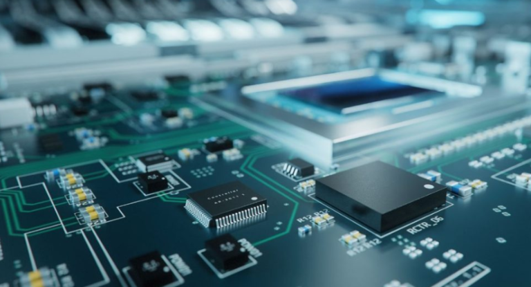
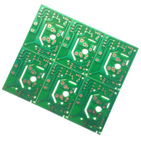
The assembly of a main controller printed circuit board (PCB) is a critical process in the manufacturing of electronic devices, serving as the backbone that supports and connects various electronic components. Understanding the basics of this assembly process is essential for anyone involved in electronics design and manufacturing. At its core, the main controller PCB assembly involves several key steps, each of which plays a vital role in ensuring the functionality and reliability of the final product.
Initially, the process begins with the design phase, where engineers create a schematic diagram that outlines the electrical connections and components required for the PCB.
This schematic is then translated into a layout design, which specifies the physical placement of components on the board. The layout design is crucial, as it must consider factors such as signal integrity, thermal management, and manufacturability. Once the design is finalized, it is sent to a fabrication facility where the PCB is manufactured. This involves creating the board’s layers, etching the copper traces, and drilling holes for component leads.
Following fabrication, the assembly process commences with the application of solder paste to the board.
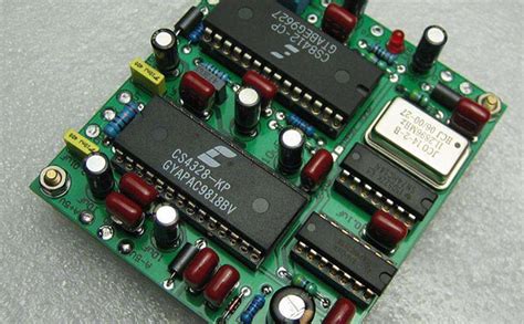
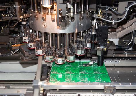
Solder paste, a mixture of powdered solder and flux, is applied to the areas where components will be mounted. This is typically done using a stencil that ensures precise application. Subsequently, components are placed onto the board using automated pick-and-place machines, which position each component with high accuracy. The components used in a main controller PCB can range from simple resistors and capacitors to complex integrated circuits and microcontrollers.
Once all components are placed, the board undergoes a reflow soldering process.
During reflow, the board is heated in a controlled environment, causing the solder paste to melt and form solid electrical connections between the components and the board. This step is critical, as it ensures that all components are securely attached and that electrical connections are reliable. After reflow, the board is inspected for any defects, such as solder bridges or misaligned components, which could affect performance.
In addition to reflow soldering, some assemblies may require through-hole components, which are inserted into pre-drilled holes and soldered manually or using wave soldering techniques. This step is often necessary for components that require a stronger mechanical bond or for those that cannot withstand the high temperatures of reflow soldering.
Quality control is an integral part of the main controller PCB assembly process.
Each board is subjected to rigorous testing to verify its functionality and performance. This may include visual inspections, automated optical inspections (AOI), and electrical testing to ensure that the board meets design specifications and operates as intended. Any defects identified during testing are addressed through rework or repair processes.
In conclusion, the assembly of a main controller PCB is a complex and meticulous process that requires careful attention to detail at every stage. From design and fabrication to component placement and soldering, each step is crucial in producing a reliable and efficient electronic device. Understanding these basics not only highlights the intricacies involved but also underscores the importance of precision and quality control in the world of electronics manufacturing. As technology continues to advance, the demand for sophisticated and reliable PCBs will only grow, making expertise in this area increasingly valuable.
Key Challenges In Main Controller PCB Assembly And How To Overcome Them
The assembly of a main controller printed circuit board (PCB) is a critical process in the manufacturing of electronic devices, serving as the central hub for controlling various functions. However, this process is fraught with challenges that can impact the performance and reliability of the final product. Understanding these challenges and implementing strategies to overcome them is essential for ensuring high-quality PCB assemblies.
One of the primary challenges in main controller PCB assembly is the complexity of the design.
electronic devices become more sophisticated, the PCBs that control them must accommodate a greater number of components and connections. This increased complexity can lead to difficulties in layout design, where ensuring optimal placement of components is crucial to avoid signal interference and maintain electrical integrity. To address this, designers can utilize advanced computer-aided design (CAD) tools that offer simulation capabilities, allowing them to test and refine layouts before physical assembly begins. This proactive approach helps in identifying potential issues early in the design phase, reducing the likelihood of costly revisions later.
Another significant challenge is the miniaturization of components.
As consumer demand for smaller, more portable devices grows, manufacturers are compelled to use increasingly smaller components on their PCBs. This miniaturization can complicate the assembly process, as precise placement and soldering of tiny components require specialized equipment and techniques. To overcome this, manufacturers can invest in automated assembly machines that offer high precision and repeatability, ensuring that even the smallest components are accurately placed and soldered. Additionally, implementing rigorous quality control measures, such as automated optical inspection (AOI) and X-ray inspection, can help detect assembly defects that may not be visible to the naked eye.
Thermal management is another critical issue in main controller PCB assembly.
As electronic components operate, they generate heat, which can lead to performance degradation or failure if not properly managed. Effective thermal management involves designing PCBs with adequate heat dissipation pathways, such as thermal vias and heat sinks, to prevent overheating. Moreover, selecting materials with high thermal conductivity for the PCB substrate can enhance heat dissipation. Manufacturers can also employ thermal simulation software during the design phase to predict heat distribution and make necessary adjustments to the layout.
Supply chain disruptions pose yet another challenge in PCB assembly.
The availability of components can be affected by various factors, including geopolitical tensions, natural disasters, and global pandemics. These disruptions can lead to delays in production and increased costs. To mitigate this risk, manufacturers can adopt a multi-sourcing strategy, securing components from multiple suppliers to ensure a steady supply. Additionally, maintaining a buffer stock of critical components can provide a cushion against unexpected supply chain interruptions.
Finally, ensuring compliance with industry standards and regulations is essential in main controller PCB assembly.
Non-compliance can result in product recalls, legal penalties, and damage to a company’s reputation. Manufacturers must stay informed about relevant standards, such as IPC standards for PCB design and assembly, and implement processes to ensure adherence. Regular training for staff on compliance requirements and conducting audits can further reinforce compliance efforts.
In conclusion, while the assembly of main controller PCBs presents several challenges, these can be effectively managed through strategic planning and the adoption of advanced technologies. By addressing design complexity, component miniaturization, thermal management, supply chain disruptions, and compliance, manufacturers can enhance the quality and reliability of their PCB assemblies, ultimately leading to more successful electronic products.
Innovations In Main Controller PCB Assembly Techniques
In recent years, the field of main controller PCB (Printed Circuit Board) assembly has witnessed significant innovations, driven by the increasing demand for more efficient, compact, and reliable electronic devices. As technology continues to evolve, the methods and techniques used in PCB assembly have had to adapt to meet the growing complexity and miniaturization of electronic components. This article explores some of the key innovations in main controller PCB assembly techniques, highlighting how these advancements are shaping the future of electronics manufacturing.
To begin with, one of the most notable innovations in PCB assembly is the adoption of surface mount technology (SMT).
Unlike traditional through-hole technology, which requires components to be inserted into drilled holes on the PCB, SMT allows components to be mounted directly onto the surface of the board. This technique not only reduces the size and weight of the final product but also enhances the performance and reliability of the electronic device. By eliminating the need for drilled holes, SMT enables higher component density and more complex circuit designs, which are essential for modern electronic applications.
In addition to SMT, the use of automated assembly processes has revolutionized the way PCBs are manufactured.
Automation in PCB assembly involves the use of sophisticated machinery and robotics to place and solder components onto the board with high precision and speed. This not only increases production efficiency but also minimizes human error, leading to higher quality and consistency in the final product. Moreover, automated assembly processes are highly adaptable, allowing manufacturers to quickly switch between different product designs and specifications, thereby reducing lead times and increasing flexibility in production.
Another significant advancement in main controller PCB assembly is the development of advanced soldering techniques.
Traditional soldering methods, such as wave soldering, are being replaced by more efficient and precise techniques like reflow soldering and selective soldering. Reflow soldering, for instance, involves the use of a controlled heat source to melt solder paste and create strong, reliable connections between components and the PCB. This method is particularly well-suited for SMT, as it allows for the simultaneous soldering of multiple components, further enhancing production efficiency.
Furthermore, the integration of advanced inspection and testing technologies has greatly improved the quality control process in PCB assembly.
Techniques such as automated optical inspection (AOI) and X-ray inspection are now commonly used to detect defects and ensure the integrity of solder joints and component placements. These technologies provide manufacturers with real-time feedback, enabling them to identify and rectify issues early in the production process, thereby reducing waste and improving overall product quality.
As we look to the future, the continued development of materials and processes will likely lead to even more innovations in main controller PCB assembly.
For instance, the use of flexible PCBs, which can be bent and shaped to fit into compact spaces, is becoming increasingly popular in applications such as wearable technology and medical devices. Additionally, advancements in materials science are paving the way for the use of environmentally friendly and sustainable materials in PCB manufacturing, aligning with the growing emphasis on green technology.
In conclusion, the innovations in main controller PCB assembly techniques are playing a crucial role in advancing the capabilities of modern electronic devices. Through the adoption of surface mount technology, automation, advanced soldering methods, and cutting-edge inspection technologies, manufacturers are able to produce smaller, more efficient, and more reliable PCBs. As technology continues to progress, these innovations will undoubtedly drive further advancements in the electronics industry, shaping the future of how we design and manufacture electronic devices.
Quality Assurance Practices In Main Controller PCB Assembly
In the realm of electronics manufacturing, the assembly of the main controller printed circuit board (PCB) is a critical process that demands meticulous attention to quality assurance practices. Ensuring the reliability and functionality of these PCBs is paramount, as they serve as the central hub for controlling various electronic devices. Consequently, manufacturers must implement rigorous quality assurance measures to maintain high standards and meet industry requirements.
To begin with, the selection of materials plays a crucial role in the quality assurance of main controller PCB assembly.
High-quality substrates, copper foils, and solder masks are essential to ensure the durability and performance of the PCB. By choosing materials that meet industry standards, manufacturers can prevent issues such as delamination, warping, and electrical failures. Furthermore, sourcing components from reputable suppliers helps in minimizing the risk of counterfeit parts, which can compromise the integrity of the entire assembly.
Transitioning from material selection, the design phase is another critical aspect of quality assurance.
A well-designed PCB layout not only optimizes the performance of the main controller but also facilitates efficient manufacturing processes. Design for manufacturability (DFM) principles should be employed to ensure that the PCB can be produced with minimal errors and rework. This includes considerations such as component placement, trace routing, and thermal management. By addressing potential design issues early in the process, manufacturers can reduce the likelihood of defects during assembly.
Once the design is finalized, the focus shifts to the assembly process itself.
Surface mount technology (SMT) and through-hole technology (THT) are commonly used methods for assembling components onto the PCB. Each method requires precise control over parameters such as temperature, pressure, and time to ensure proper soldering and component placement. Automated optical inspection (AOI) systems are often employed to verify the accuracy of component placement and solder joints, providing an additional layer of quality assurance.
In addition to automated inspections, manual inspections are also crucial in identifying defects that machines may overlook.
Skilled technicians perform visual inspections to detect issues such as solder bridges, misaligned components, and insufficient solder coverage. These inspections are complemented by functional testing, where the assembled PCB is subjected to various electrical tests to verify its performance. Functional testing ensures that the main controller operates as intended and meets the specified requirements.
Moreover, environmental testing is an integral part of quality assurance in main controller PCB assembly.
PCBs are often exposed to harsh conditions, such as extreme temperatures, humidity, and vibrations. Environmental testing simulates these conditions to evaluate the PCB’s resilience and reliability. By subjecting the PCB to rigorous testing, manufacturers can identify potential weaknesses and make necessary improvements to enhance its durability.
Finally, continuous improvement is a cornerstone of quality assurance practices in main controller PCB assembly.
Manufacturers must regularly review and update their processes to incorporate the latest advancements in technology and industry standards. This includes investing in employee training, upgrading equipment, and implementing feedback loops to capture insights from previous projects. By fostering a culture of continuous improvement, manufacturers can consistently deliver high-quality PCBs that meet the evolving demands of the electronics industry.
In conclusion, quality assurance practices in main controller PCB assembly encompass a comprehensive approach that spans material selection, design, assembly, inspection, testing, and continuous improvement. By adhering to these practices, manufacturers can ensure the production of reliable and high-performing PCBs that serve as the backbone of modern electronic devices.