Main PCB Assembly: The Heart of Modern Electronics
Introduction
Printed Circuit Board (PCB) assembly is a critical process in the manufacturing of electronic devices. Among the various types of PCB assemblies, the Main PCB Assembly (Main PCBA) serves as the core component in most electronic systems, housing essential circuits, processors, memory modules, and power distribution networks. This article explores the significance of Main PCB Assembly, its components, manufacturing processes, challenges, and future trends.
1. What is a Main PCB Assembly?
The Main PCB Assembly is the primary circuit board in an electronic device, integrating key functionalities such as processing, power management, and connectivity. It acts as the central hub, connecting all peripheral components and ensuring seamless operation. Examples include:
- Motherboards in computers and servers
- Main control boards in smartphones and tablets
- System boards in automotive electronics and industrial machines
Unlike auxiliary PCBs (e.g., power supply boards or sensor modules), the Main PCBA is responsible for the device’s core operations.
2. Key Components of a Main PCB Assembly
A typical Main PCBA consists of several critical components:
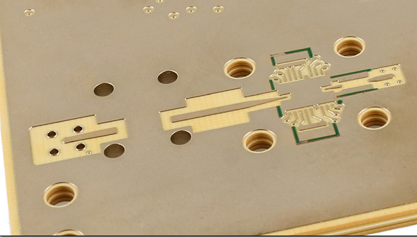
2.1. Substrate (PCB Base Material)
- Made of FR-4 (Flame Retardant-4) or high-frequency laminates (e.g., Rogers or Teflon for RF applications).
- Multi-layer designs (4 to 20+ layers) for complex circuits.
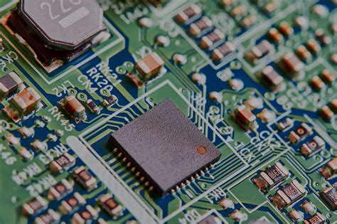
2.2. Integrated Circuits (ICs)
- Microprocessors & Microcontrollers (e.g., Intel CPUs, ARM Cortex chips).
- Memory Modules (DRAM, Flash, EEPROM).
- FPGAs & ASICs for specialized processing.
2.3. Passive Components
- Resistors, Capacitors, Inductors for signal conditioning.
- Oscillators & Crystal Resonators for clock generation.
2.4. Connectors & Interfaces
- USB, HDMI, PCIe, M.2 for external connections.
- Power Connectors (e.g., ATX in motherboards).
2.5. Power Management ICs (PMICs)
- Voltage regulators (LDOs, Buck/Boost converters).
- Battery management systems (for portable devices).
2.6. RF & Wireless Modules
- Wi-Fi, Bluetooth, 5G modems in smartphones.
- GPS & NFC modules for location and connectivity.
3. The Main PCB Assembly Process
The manufacturing of a Main PCBA involves several stages:
3.1. PCB Fabrication
- Design & Layout: Using CAD tools like Altium Designer or KiCad.
- Layer Stackup: Determining copper layers and dielectric materials.
- Etching & Drilling: Creating conductive traces and vias.
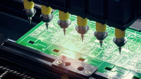
3.2. Component Placement
- Surface Mount Technology (SMT): Automated pick-and-place machines position tiny components.
- Through-Hole Technology (THT): For larger components like connectors.
3.3. Soldering
- Reflow Soldering (for SMT): Heating the board to melt solder paste.
- Wave Soldering (for THT): Passing the PCB over a molten solder wave.
3.4. Inspection & Testing
- Automated Optical Inspection (AOI): Detects soldering defects.
- In-Circuit Testing (ICT): Validates electrical connections.
- Functional Testing: Ensures the board operates as intended.
3.5. Conformal Coating & Enclosure Assembly
- Protects against moisture, dust, and corrosion.
- Final integration into the device chassis.
4. Challenges in Main PCB Assembly
Despite advancements, manufacturers face several challenges:
4.1. Miniaturization & High-Density Designs
- Shrinking component sizes (e.g., 01005 resistors) require precision assembly.
- High-speed signal integrity issues (e.g., impedance control in DDR5 traces).
4.2. Thermal Management
- High-power CPUs and GPUs generate heat, requiring efficient cooling solutions.
- Thermal vias and heat sinks are integrated into the PCB design.
4.3. Supply Chain & Component Shortages
- Global chip shortages impact Main PCBA production.
- Long lead times for specialized ICs (e.g., automotive-grade MCUs).
4.4. Reliability & Durability
- Automotive and aerospace PCBAs must withstand extreme conditions.
- Conformal coating and ruggedized designs improve longevity.
5. Future Trends in Main PCB Assembly
5.1. High-Speed & 5G PCBs
- Increased demand for low-loss materials (PTFE, ceramic-filled laminates).
- Millimeter-wave (mmWave) PCBs for 5G and radar applications.
5.2. AI & Edge Computing Integration
- Main PCBAs will incorporate AI accelerators (e.g., NPUs).
- Edge devices require low-power, high-performance designs.
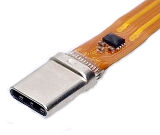
5.3. Flexible & Rigid-Flex PCBs
- Wearables and foldable smartphones use flexible PCB assemblies.
5.4. Sustainable Manufacturing
- Lead-free soldering and recyclable materials.
- Energy-efficient production techniques.
Conclusion
The Main PCB Assembly is the backbone of modern electronics, enabling everything from consumer gadgets to industrial automation. As technology evolves, the demand for high-performance, compact, and reliable Main PCBAs will continue to grow. Manufacturers must adapt to new materials, advanced assembly techniques, and supply chain challenges to meet these demands.
With innovations in 5G, AI, and flexible electronics, the future of Main PCB Assembly promises even greater integration and functionality, shaping the next generation of smart devices.