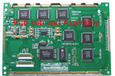
Make pcb online
Step-by-Step Guide to Designing Your First PCB Online
Designing your first printed circuit board (PCB) online can be an exciting yet daunting task. However, with the right guidance and tools, the process can be streamlined and accessible even for beginners. The advent of online PCB design platforms has revolutionized the way hobbyists and professionals alike approach electronic design, offering a range of features that simplify the creation of complex circuits. This guide will walk you through the essential steps to design your first PCB online, ensuring a smooth transition from concept to creation.
To begin with, selecting the right online PCB design software is crucial.
Numerous platforms are available, each offering unique features tailored to different needs. Popular options include EasyEDA, KiCad, and Altium Designer. These platforms provide user-friendly interfaces and extensive libraries of components, making it easier to bring your ideas to life. Once you have chosen a platform, the next step is to familiarize yourself with its interface and tools. Most platforms offer tutorials and documentation to help you get started, which can be invaluable for understanding the basic functionalities.
After setting up your design environment, the next phase involves creating a schematic diagram.
This step is fundamental as it represents the electrical connections between different components in your circuit. Begin by selecting the components you need from the software’s library and placing them on the schematic canvas. It is essential to ensure that each component is correctly labeled and connected, as this will directly impact the functionality of your PCB. As you work through this process, take advantage of the software’s simulation features to test your circuit design. This can help identify potential issues before moving on to the next stage.
Once your schematic is complete and verified, the next step is to convert it into a PCB layout.
This involves arranging the physical components on a board and routing the electrical connections between them. Online PCB design tools typically offer auto-routing features, which can significantly speed up this process. However, manual routing may be necessary for more complex designs to optimize the layout and minimize interference. During this stage, it is important to consider factors such as component placement, trace width, and layer management to ensure a functional and manufacturable PCB.
With your PCB layout finalized, the next step is to generate the necessary files for manufacturing.
These files, commonly known as Gerber files, contain all the information required to produce your PCB. Most online design platforms offer built-in tools to generate these files, ensuring they meet industry standards. It is advisable to review these files carefully to avoid any errors that could affect the manufacturing process.
Finally, once your design files are ready, you can proceed to order your PCB from a manufacturer.
Many online platforms are integrated with PCB fabrication services, allowing you to upload your files and receive a quote instantly. When selecting a manufacturer, consider factors such as turnaround time, cost, and quality to ensure your final product meets your expectations.
In conclusion, designing your first PCB online involves a series of well-defined steps, from selecting the right software to finalizing your design for manufacturing. By following this guide and utilizing the resources available through online platforms, you can successfully navigate the process and bring your electronic projects to fruition.

Top Online Tools for PCB Design and Prototyping
In the rapidly evolving world of electronics, the ability to design and prototype printed circuit boards (PCBs) online has become an invaluable asset for engineers, hobbyists, and startups alike. The convenience and accessibility of online tools have revolutionized the way PCBs are created, allowing for faster iterations and more efficient workflows. As the demand for custom electronics grows, so does the need for reliable and user-friendly online platforms that cater to PCB design and prototyping. This article explores some of the top online tools available today, highlighting their features and benefits to help you make an informed choice.
One of the most popular online tools for PCB design is EasyEDA.
This platform offers a comprehensive suite of features that cater to both beginners and experienced designers. With its intuitive interface, EasyEDA allows users to create schematics, simulate circuits, and design PCBs with ease. Moreover, it provides a vast library of components, which simplifies the process of selecting and placing parts on the board. The integration with LCSC, a major electronic component supplier, further enhances its appeal by streamlining the component sourcing process. Additionally, EasyEDA supports collaboration, enabling multiple users to work on a project simultaneously, which is particularly beneficial for team-based projects.
Another noteworthy tool is KiCad, an open-source software that has gained a strong following due to its robust capabilities and active community support.
Although traditionally a desktop application, KiCad has made strides in offering online functionalities that enhance its usability. It provides a powerful set of features, including a schematic editor, PCB layout tool, and 3D viewer, which together facilitate the creation of complex designs. The open-source nature of KiCad means that users can customize the software to suit their specific needs, and the extensive documentation and community forums offer valuable resources for troubleshooting and learning.
For those seeking a more integrated approach, Altium 365 offers a cloud-based platform that combines design, collaboration, and manufacturing in one seamless environment.
Altium 365 allows users to access their projects from anywhere, making it ideal for remote teams and individuals who require flexibility. The platform’s advanced features, such as real-time collaboration and version control, ensure that all stakeholders are aligned throughout the design process. Furthermore, Altium 365’s integration with manufacturing partners enables a smooth transition from design to production, reducing the time and effort required to bring a product to market.
In addition to these tools, Upverter stands out as a unique option for those interested in open-source hardware design.
Upverter’s browser-based platform emphasizes collaboration and community-driven development, allowing users to share and remix designs with ease. This approach fosters innovation and accelerates the development of new ideas, making it an attractive choice for makers and startups looking to leverage collective expertise.
As we consider the landscape of online PCB design tools, it is clear that each platform offers distinct advantages tailored to different user needs. Whether you prioritize ease of use, advanced features, or community engagement, there is a tool that can meet your requirements. By leveraging these online resources, designers can streamline their workflows, reduce costs, and ultimately bring their electronic innovations to life more efficiently. As technology continues to advance, the capabilities of these tools will undoubtedly expand, further enhancing the possibilities for PCB design and prototyping in the digital age.
Benefits of Using Online Platforms for PCB Manufacturing
In recent years, the advent of online platforms for printed circuit board (PCB) manufacturing has revolutionized the electronics industry, offering numerous benefits that cater to both hobbyists and professional engineers. One of the most significant advantages of using online platforms for PCB manufacturing is the accessibility they provide. Traditionally, PCB manufacturing required a substantial investment in equipment and materials, which often posed a barrier to entry for small businesses and individual innovators. However, online platforms have democratized access to PCB manufacturing by allowing users to design and order PCBs without the need for expensive machinery or extensive technical expertise.
Moreover, these platforms offer a high degree of convenience, enabling users to design PCBs from the comfort of their own homes or offices.
With user-friendly interfaces and comprehensive design tools, individuals can create complex PCB layouts with relative ease. This convenience is further enhanced by the ability to upload designs directly to the platform, where they can be reviewed and modified as needed. As a result, the entire process, from design to production, is streamlined, saving both time and effort.
In addition to accessibility and convenience, online PCB manufacturing platforms provide a level of flexibility that is unmatched by traditional methods.
Users can choose from a wide range of materials, finishes, and specifications to suit their specific needs. This customization ensures that the final product meets the exact requirements of the project, whether it is for a simple prototype or a complex, multi-layered board. Furthermore, many platforms offer rapid prototyping services, allowing users to quickly test and iterate their designs. This agility is crucial in today’s fast-paced technological landscape, where the ability to adapt and innovate is key to staying competitive.
Another notable benefit of using online platforms for PCB manufacturing is the cost-effectiveness they offer.
By eliminating the need for physical infrastructure and reducing labor costs, these platforms can provide high-quality PCBs at a fraction of the cost of traditional manufacturing methods. Additionally, many platforms offer tiered pricing structures, enabling users to select options that fit their budget. This affordability makes it feasible for startups and small businesses to bring their products to market without incurring prohibitive expenses.
Furthermore, online PCB manufacturing platforms often incorporate advanced technologies such as automated design rule checks and real-time feedback, which enhance the accuracy and reliability of the final product.
These features help to minimize errors and ensure that the PCBs function as intended, reducing the likelihood of costly revisions or rework. The integration of such technologies not only improves the quality of the PCBs but also instills confidence in users, knowing that their designs are being handled with precision and care.
In conclusion, the benefits of using online platforms for PCB manufacturing are manifold, encompassing accessibility, convenience, flexibility, cost-effectiveness, and technological sophistication. As the electronics industry continues to evolve, these platforms are poised to play an increasingly vital role in facilitating innovation and enabling creators to bring their ideas to life. By leveraging the advantages offered by online PCB manufacturing, individuals and businesses alike can overcome traditional barriers and contribute to the advancement of technology in meaningful ways.
Common Mistakes to Avoid When Creating PCBs Online
Creating printed circuit boards (PCBs) online has become increasingly accessible, thanks to advancements in technology and the availability of user-friendly design software. However, despite these conveniences, there are common mistakes that can occur during the design and ordering process. Understanding these pitfalls is crucial for both novice and experienced designers to ensure the production of high-quality PCBs.
One frequent mistake is neglecting to thoroughly review the design rules and specifications provided by the PCB manufacturer.
Each manufacturer may have unique requirements regarding trace width, spacing, and layer stack-up. Failing to adhere to these guidelines can result in a design that is either unmanufacturable or requires costly revisions. Therefore, it is essential to consult the manufacturer’s design rules early in the design process and incorporate them into your project.
Another common error is overlooking the importance of component placement and routing.
Efficient component placement is vital for optimal circuit performance and ease of assembly. Poor placement can lead to increased signal interference, longer trace lengths, and potential thermal issues. To avoid these problems, designers should prioritize placing components with high connectivity close to each other and consider the flow of signals through the board. Additionally, using a grid system can help maintain alignment and organization.
Transitioning to the topic of routing, it is crucial to avoid creating traces that are too narrow or too close together.
Narrow traces can lead to increased resistance and potential overheating, while traces that are too close can cause short circuits. Utilizing the design rule check (DRC) feature in PCB design software can help identify these issues before the design is finalized. Moreover, designers should be mindful of trace angles, avoiding acute angles that can cause signal reflection and impedance mismatches.
Furthermore, neglecting to include adequate thermal management features is a mistake that can compromise the reliability of the PCB.
Components that generate significant heat require proper heat dissipation strategies, such as thermal vias, heat sinks, or copper pours. Failing to address thermal management can lead to component failure and reduced lifespan of the PCB. Therefore, it is advisable to conduct thermal simulations during the design phase to identify potential hotspots and implement appropriate cooling solutions.
In addition to technical considerations, designers must also pay attention to the documentation accompanying their PCB design.
Incomplete or unclear documentation can lead to misunderstandings and errors during manufacturing. It is important to provide detailed fabrication and assembly drawings, including layer stack-up information, drill files, and a bill of materials (BOM). Clear documentation ensures that the manufacturer has all the necessary information to produce the PCB accurately.
Finally, a common oversight is not performing a comprehensive review of the final design before submission.
This review should include checking for any unconnected nets, verifying component footprints, and ensuring that all design rule violations have been addressed. Taking the time to conduct a thorough review can prevent costly mistakes and delays in production.
In conclusion, while creating PCBs online offers numerous advantages, it is essential to be aware of common mistakes that can occur during the design process. By adhering to manufacturer specifications, optimizing component placement and routing, addressing thermal management, providing clear documentation, and conducting a final design review, designers can significantly improve the quality and reliability of their PCBs.