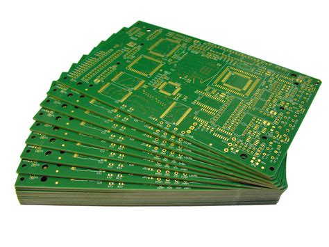
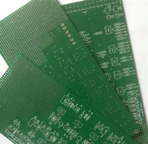
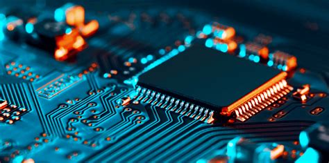
Manufacturing pcbs
Innovations In PCB Manufacturing Techniques
In recent years, the field of printed circuit board (PCB) manufacturing has witnessed a series of innovative advancements that have significantly transformed the industry. These innovations are not only enhancing the efficiency and precision of PCB production but are also paving the way for more complex and compact electronic devices. As the demand for smaller, faster, and more reliable electronic products continues to grow, manufacturers are increasingly adopting cutting-edge techniques to meet these evolving needs.
One of the most notable innovations in PCB manufacturing is the advent of advanced materials.
Traditionally, PCBs were primarily made from fiberglass-reinforced epoxy laminates, which, while effective, had limitations in terms of thermal management and signal integrity. Today, manufacturers are exploring alternative materials such as ceramic substrates and metal-core PCBs. These materials offer superior thermal conductivity and mechanical stability, making them ideal for high-performance applications. By utilizing these advanced materials, manufacturers can produce PCBs that are not only more durable but also capable of supporting higher power densities.
In addition to material advancements, the integration of automation and robotics in PCB manufacturing has revolutionized the production process.
Automated systems are now capable of performing intricate tasks with remarkable precision, reducing the likelihood of human error and increasing overall production efficiency. For instance, automated optical inspection (AOI) systems are employed to meticulously examine PCBs for defects, ensuring that only high-quality products reach the market. Furthermore, robotic assembly lines have streamlined the soldering and component placement processes, allowing for faster production times and reduced labor costs.
Another significant innovation is the implementation of additive manufacturing techniques, commonly known as 3D printing, in PCB production.
This approach allows for the creation of complex, multi-layered PCBs with intricate geometries that would be challenging to achieve using traditional subtractive methods. By building PCBs layer by layer, manufacturers can optimize the use of materials and minimize waste, leading to more sustainable production practices. Moreover, 3D printing enables rapid prototyping, allowing designers to quickly iterate and refine their designs before committing to full-scale production.
The rise of Internet of Things (IoT) devices has also driven the need for flexible and wearable PCBs.
To address this demand, manufacturers are developing flexible PCBs that can bend and conform to various shapes without compromising functionality. These flexible circuits are made possible through the use of innovative materials such as polyimide films and conductive inks, which provide the necessary flexibility and conductivity. As a result, flexible PCBs are becoming increasingly prevalent in applications ranging from medical devices to consumer electronics.
Furthermore, advancements in PCB design software have played a crucial role in facilitating these manufacturing innovations.
Modern design tools offer sophisticated simulation and analysis capabilities, enabling engineers to optimize their designs for performance, manufacturability, and cost-effectiveness. By leveraging these tools, designers can predict potential issues and make informed decisions early in the design process, ultimately leading to more reliable and efficient PCBs.
In conclusion, the landscape of PCB manufacturing is undergoing a remarkable transformation driven by innovations in materials, automation, additive manufacturing, and design software. These advancements are not only enhancing the capabilities of PCBs but are also enabling the development of next-generation electronic devices. As technology continues to evolve, it is clear that the future of PCB manufacturing will be characterized by even greater levels of precision, efficiency, and sustainability.
The Role Of Automation In PCB Production
In the rapidly evolving landscape of electronics manufacturing, the role of automation in printed circuit board (PCB) production has become increasingly significant. As the demand for more complex and miniaturized electronic devices grows, manufacturers are compelled to adopt advanced technologies to enhance efficiency, precision, and scalability. Automation, in this context, serves as a pivotal force driving the transformation of PCB production processes, offering numerous advantages that are reshaping the industry.
To begin with, automation in PCB manufacturing significantly enhances production efficiency.
Traditional manual methods are often labor-intensive and time-consuming, leading to potential bottlenecks in the production line. By integrating automated systems, manufacturers can streamline operations, reducing the time required for each production cycle. Automated machines can operate continuously with minimal human intervention, thereby increasing throughput and enabling manufacturers to meet tight deadlines and high-volume demands. This efficiency is particularly crucial in an era where time-to-market is a critical factor for competitive advantage.
Moreover, automation ensures a higher degree of precision and consistency in PCB production. Human error, an inherent risk in manual processes, can lead to defects and inconsistencies in the final product. Automated systems, on the other hand, are programmed to perform tasks with exacting accuracy, ensuring that each PCB is produced to the same specifications. This precision is vital for maintaining the quality and reliability of electronic devices, especially as PCBs become more intricate with the integration of advanced components and technologies.
In addition to efficiency and precision, automation also contributes to cost-effectiveness in PCB manufacturing.
While the initial investment in automated equipment can be substantial, the long-term savings are significant. Automation reduces the need for a large workforce, thereby lowering labor costs. Furthermore, the reduction in errors and defects minimizes waste and rework, leading to more efficient use of materials and resources. Over time, these savings can offset the initial capital expenditure, making automation a financially viable option for many manufacturers.
Transitioning to the environmental impact, automation in PCB production also supports sustainability efforts.
Automated systems are often designed to optimize resource usage, reducing energy consumption and minimizing waste. For instance, precision in material application ensures that only the necessary amount of solder or adhesive is used, reducing excess and preventing environmental contamination. Additionally, automated processes can be more easily monitored and controlled, allowing manufacturers to implement eco-friendly practices and comply with environmental regulations more effectively.
Furthermore, the integration of automation in PCB production facilitates innovation and adaptability.
As technology continues to advance, manufacturers must be able to quickly adapt to new trends and requirements. Automated systems can be reprogrammed and reconfigured to accommodate changes in design and production needs, providing the flexibility necessary to stay ahead in a competitive market. This adaptability is crucial for manufacturers looking to innovate and develop cutting-edge products that meet the evolving demands of consumers.
In conclusion, the role of automation in PCB production is multifaceted, offering benefits that extend beyond mere efficiency gains. By enhancing precision, reducing costs, supporting sustainability, and enabling adaptability, automation is transforming the PCB manufacturing industry. As technology continues to advance, the integration of automated systems will undoubtedly play an even more critical role in shaping the future of electronics manufacturing, driving progress and innovation in ways that were once unimaginable.
Environmental Impact Of PCB Manufacturing
The manufacturing of printed circuit boards (PCBs) is a critical component of the electronics industry, serving as the backbone for a multitude of electronic devices. However, this process is not without its environmental implications. Understanding the environmental impact of PCB manufacturing is essential for developing strategies to mitigate its adverse effects and promote sustainable practices within the industry.
To begin with, the production of PCBs involves several stages, each contributing to environmental concerns.
The initial phase includes the creation of the substrate, typically made from fiberglass reinforced with epoxy resin. This process requires significant energy consumption and the use of chemicals that can be harmful if not managed properly. The extraction and processing of raw materials, such as copper, also contribute to environmental degradation, including habitat destruction and pollution.
Moreover, the etching process, which is used to create the circuit patterns on the board, involves the use of corrosive chemicals like ferric chloride and ammonium persulfate.
These substances, if not disposed of correctly, can lead to soil and water contamination. The improper handling of these chemicals poses a risk not only to the environment but also to human health, as they can leach into groundwater supplies and affect local ecosystems.
In addition to chemical waste, PCB manufacturing generates a significant amount of solid waste.
This includes off-cuts from the boards, defective units, and packaging materials. The disposal of these materials in landfills contributes to the growing problem of electronic waste, which is a major environmental concern due to its non-biodegradable nature and the presence of toxic substances.
Furthermore, the energy-intensive nature of PCB production results in substantial greenhouse gas emissions.
The reliance on fossil fuels for energy in many manufacturing facilities exacerbates the issue of climate change. As the demand for electronic devices continues to rise, so too does the pressure on manufacturers to find more energy-efficient and environmentally friendly production methods.
Transitioning to more sustainable practices in PCB manufacturing is not only beneficial for the environment but also economically advantageous in the long run.
Companies are increasingly adopting green manufacturing techniques, such as using water-based solvents instead of traditional chemical etchants and implementing closed-loop systems to recycle water and reduce waste. Additionally, advancements in technology have led to the development of alternative materials, such as biodegradable substrates, which can significantly reduce the environmental footprint of PCBs.
Regulatory frameworks also play a crucial role in minimizing the environmental impact of PCB manufacturing.
Governments worldwide are implementing stricter regulations on waste management and emissions, encouraging companies to adopt cleaner production methods. Compliance with these regulations not only helps protect the environment but also enhances a company’s reputation and competitiveness in the global market.
In conclusion, while PCB manufacturing is indispensable to the electronics industry, it is imperative to address its environmental impact. By adopting sustainable practices, investing in research and development for eco-friendly materials, and adhering to regulatory standards, the industry can significantly reduce its ecological footprint. As awareness of environmental issues continues to grow, the shift towards greener manufacturing processes will not only benefit the planet but also ensure the long-term viability of the industry.
Quality Control Measures In PCB Fabrication
In the intricate world of electronics, printed circuit boards (PCBs) serve as the backbone of most devices, facilitating the connection and communication between various components. As the demand for more sophisticated and reliable electronic devices grows, the importance of quality control in PCB fabrication becomes increasingly paramount. Ensuring the highest standards of quality not only enhances the performance and longevity of electronic products but also minimizes the risk of costly failures and recalls.
To begin with, the quality control process in PCB fabrication starts with the selection of raw materials.
High-quality substrates, copper foils, and laminates are essential to ensure the durability and functionality of the final product. Manufacturers often source materials from reputable suppliers and conduct rigorous inspections to verify their compliance with industry standards. This initial step is crucial, as any compromise in material quality can lead to defects that may not be easily rectifiable later in the production process.
Following the procurement of materials, the design phase plays a critical role in quality assurance.
Advanced design software is employed to create precise and error-free PCB layouts. Design for manufacturability (DFM) checks are conducted to identify potential issues that could arise during production. These checks help in optimizing the design to ensure that it can be manufactured efficiently without compromising on quality. Moreover, design rule checks (DRC) are performed to ensure that the layout adheres to the specific requirements and constraints of the manufacturing process.
As the fabrication process commences, several quality control measures are implemented at various stages.
During the etching process, for instance, manufacturers use automated optical inspection (AOI) systems to detect any discrepancies in the etched patterns. This technology allows for the early identification of defects such as shorts, opens, and insufficient copper thickness, which can be rectified before proceeding to subsequent stages. Additionally, solder mask application and silkscreen printing are closely monitored to ensure proper alignment and adhesion, which are vital for the board’s functionality and appearance.
Another critical aspect of quality control in PCB fabrication is the testing of electrical properties.
Electrical testing, including continuity and isolation tests, is conducted to verify that the circuit paths are correctly formed and that there are no unintended connections. These tests are essential in ensuring that the PCB will perform as intended in its final application. Furthermore, impedance control is often required for high-frequency applications, necessitating precise measurements and adjustments to maintain signal integrity.
In addition to these technical measures, environmental and mechanical testing is also performed to assess the PCB’s resilience under various conditions.
cycling tests, for example, evaluate the board’s ability to withstand temperature fluctuations, while vibration tests assess its durability under mechanical stress. These tests are crucial for applications where the PCB will be exposed to harsh environments, such as in automotive or aerospace industries.
Finally, documentation and traceability are integral components of the quality control process.
Detailed records of each production batch, including material sources, test results, and inspection reports, are maintained to ensure traceability and accountability. This documentation not only facilitates troubleshooting in case of defects but also provides valuable data for continuous improvement efforts.
In conclusion, quality control measures in PCB fabrication are multifaceted and encompass every stage of the production process. From material selection and design optimization to rigorous testing and documentation, each step is meticulously executed to ensure the highest standards of quality. As technology continues to advance, the emphasis on quality control in PCB manufacturing will remain a critical factor in delivering reliable and high-performance electronic products.


