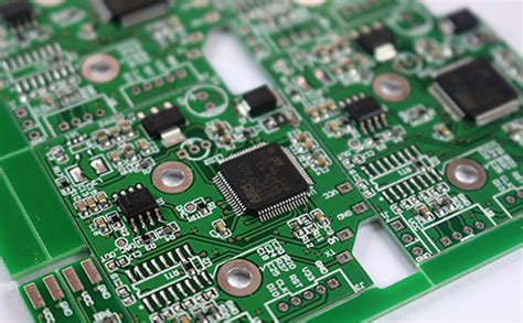
Manufacturing process knowledge that needs to be known for high-layer PCB design
As electronic devices develop towards higher performance and smaller size, their requirements for PCB precision and performance are also getting higher and higher.
High-layer PCBs can provide more routing layers, making circuit design more complex and dense, thereby meeting the needs of high-frequency and high-speed transmission. In addition, high-layer PCBs can also achieve better signal integrity and electromagnetic compatibility. This is particularly important for high-end application fields such as 5G communications, high-performance computing, and automotive electronics. Therefore, high-layer PCBs have become one of the important trends in the future development of the PCB industry. For PCB design engineers or electronic hardware design engineers, it is also necessary to understand the manufacturing process related to high-layer PCBs.
High-layer PCBs are not only an increase in the number of layers, but also a doubling of their manufacturing difficulty.
Compared with single-layer and double-layer boards, the production and manufacturing of high-layer PCBs will also need to pay attention to the control of processes such as inter-layer connection, inter-layer stacking and alignment, and precise pressing control. When designing PCBs, it is also necessary to consider issues such as signal integrity, electromagnetic interference, and thermal management to fully utilize the performance advantages of high-layer PCBs.
From process, equipment, design capabilities to quality control and collaboration capabilities, high-layer boards have higher requirements for the manufacturing process level of PCB board factories. In this article, we will introduce the design process of high-layer PCBs.
1.Submit manufacturing information
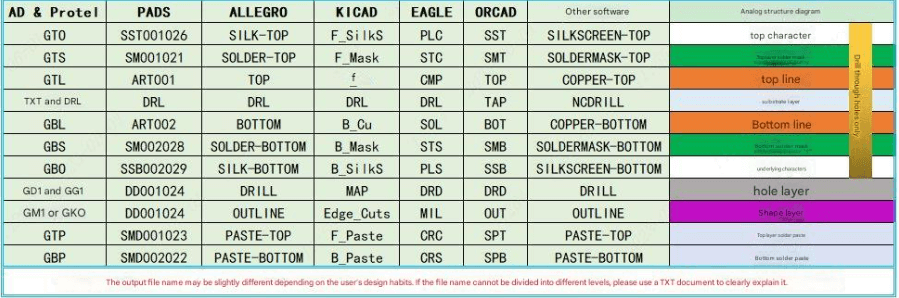
As the beginning of PCB manufacturing, first of all, we need to submit relevant manufacturing information to the PCB board factory. The information and common data formats required for PCB manufacturing include the following:
Gerber file (RS274X format)
Gerber RS274X is the current mainstream format. The output Gerber file includes all circuit layers, solder mask layers, solder paste layers, silk screen (character) layers, board frames, hole diagrams, and manufacturing requirements (such as multi-layer board stacking structure diagrams, interlayer dielectric thickness, impedance control requirements, plugging requirements, etc.). At the same time, the Gerber file must also be convenient for the process engineers of the PCB board factory to identify the layer information corresponding to each Gerber file, so it is recommended to name the Gerber file according to a certain naming convention. For example, the naming convention given by Jiali Chuang is a good reference:
Drilling file
The drilling file contains all drilling coordinates and diameter data. The commonly used file format is Excellon format.
Netlist data
IPC defines the compatible format IPC-356, which provides all the information necessary to generate netlists and electrical performance test data. Compared with single-layer or double-sided boards, complete PCB documents are very important for the manufacture of multi-layer PCBs. The most important information in the manufacturing information document is:
- Complete layer structure
- Accurate information about the substrate
- High-frequency and high-speed boards also need to provide the substrate manufacturer and product name
- Impedance control requirements
- Special process instructions (such as plugging requirements)
2.Manufacturing information review
The purpose of the PCB board factory’s review of manufacturing information is to determine the approximate manufacturing cost and prepare for manufacturing. Before product manufacturing or processing, proper preliminary analysis can save time and materials. The responsibility of the PCB board factory is to determine whether its process capabilities can meet the given product.
PCB manufacturers will adjust the wiring information of PCB design according to their manufacturing process, such as via drill diameter compensation or trace etching compensation, etc., in order to improve PCB manufacturability. Some key modifications will also be communicated and confirmed with PCB Layout. Of course, the ideal situation is that DFM manufacturability is considered and design optimization is performed during the PCB design process, which will save a lot of time for later communication and confirmation with PCB manufacturers.
3.Material preparation
Single-sided and double-sided circuit boards are directly manufactured using copper-clad laminates that meet the thickness requirements of the final product, but multi-layer circuit boards are different. Multi-layer circuit boards have multiple copper layers in the circuit board structure, so special substrates are required for manufacturing. Creating a multi-layer circuit board requires the use of prepreg (PP) and a relatively thin copper-clad laminate (Core) to form the final thickness after combination pressing and curing. The laminate structure depends on the electrical parameters, which is determined by the PCB designer and the circuit board manufacturer, and is planned in advance before PCB Layout to meet the line width/line spacing requirements of specific impedance.
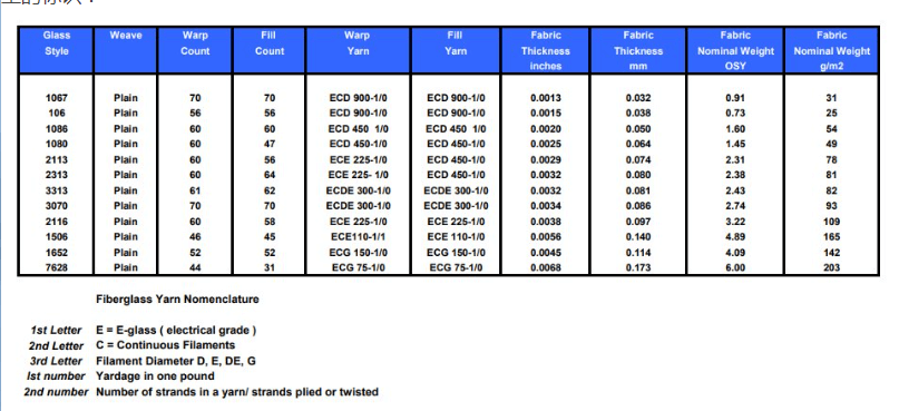
Due to different laminate structures, the thickness of the prepreg also varies to meet different transmission line and power plane combination requirements. Each prepreg is made up of a specified glass fiber weave type and is numbered, such as 1080, 2116, 3313, or 7628. The following figure shows the identification of this type:
The second component of a multilayer circuit board is a relatively thin copper-clad laminate (relative to the copper-clad laminate used to make single- and double-sided PCBs), also known as a core board. It is a fully cured substrate with copper foil on one or both sides. Of course, there are also those that do not contain copper, called bare boards.
The core board is actually also made of prepreg and copper foil laminated together, and is manufactured by the substrate supplier.
The substrate supplier will select different woven styles of glass fiber cloth and resin content prepreg according to the IPC-4101 specification and market demand, and match it with copper foil of specified specifications. After lamination, different types of copper-clad laminates are generated.

The manufacture of multi-layer circuit boards is completed by PCB board factories, but the substrate is provided by substrate manufacturers. It should be noted that there are many specifications of substrates, and the substrate reserves of each PCB board factory are also different. If the PCB stacking design requires the use of special specifications of prepregs and core boards, it is best to communicate with the PCB board factory in advance to understand the supply cycle of the substrate.
Only by selecting good raw materials can you make a PCB with excellent performance.
The board plays a key role in the PCB manufacturing process and has an important impact on the performance and reliability of the PCB, including electrical performance, thermal performance, mechanical strength, processing performance and environmental adaptability.
In terms of board materials, Jiali Chuang uses raw materials from large factories. For 4-layer boards and 6-layer boards, Jiali Chuang uses KB and Nan Ya boards from Taiwan, China, which are of high quality and guaranteed. KB board materials use high-quality glass fiber reinforced epoxy resin (FR-4) as the substrate, high-purity copper foil as the conductive layer, and undergo strict process treatment. Therefore, they have the characteristics of high quality and good performance and are widely used in the electronics industry.
Nan Ya of Taiwan, China is also well-known in the market.
The sheets it provides not only have good electrical properties, high strength and rigidity, but also high temperature resistance and chemical resistance, which can improve the reliability and life of the product.
For 8-layer boards and higher, Jiali Chuang uses Nan Ya of Taiwan, China and Shengyi sheets. Among them, as a well-known domestic copper clad laminate supplier, Shengyi sheets have the characteristics of high standards, high quality, high performance and high reliability, and are highly recognized by the industry. They are widely used in electronic products such as industrial control, medical instruments/equipment, consumer electronics, and automobiles.
4.Manufacturing process of multilayer boards
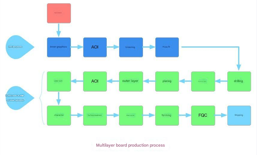
As shown in the above multilayer board production process flow, the manufacturing of multilayer boards has an additional inner layer process compared with the manufacturing of single-sided and double-sided PCBs. The key step is the control of the inner layer lamination process, which is crucial to the electrical performance of controlled impedance transmission lines. After the inner layer process is completed, it comes to the same manufacturing process flow as the manufacturing of single-sided and double-sided boards until the final inspection process.
If the production process of multilayer boards is detailed and expanded, it usually requires about 200 different processing steps. Therefore, it is very important for PCB designers to be familiar with the different types and properties of substrates, the manufacturing process of multilayer boards, and the soldering process. All required thicknesses can be achieved by combining prepregs of different specifications and copper-clad laminates (core boards).
For the stacking structure of multilayer boards, it is necessary to pay attention to the symmetry of the layers and the same layer thickness. The copper of the inner layer should be evenly distributed on these symmetrical layers.
If the distribution is uneven, the uneven thermal stress during heating will cause the circuit board to warp.
One of the factors that greatly affects the quality of the multilayer board structure is the precise adjustment between the layers.
The layers must be precisely overlapped, otherwise the circuits between the layers may have open short circuit problems after being connected by drilling. Precise adjustment is performed by mechanical alignment holes, and then the stacking is adjusted using positioning pins during stacking. In order to ensure good adhesion between the inner layers and the prepreg, the copper surface must be chemically roughened, which is called browning. Before laminating a multilayer printed circuit board, it is essential to inspect the internal circuit layer to ensure quality. At this stage, if the inspection finds connections or other defects, they can still be repaired. The inspection is usually performed automatically using AOI (automatic optical inspection). The AOI system directly compares the etched circuit pattern with the CAD data visually.
The above figure is a schematic diagram of the lamination manufacturing of a 6-layer rigid multilayer board. A1, A2, and A3 are prepregs, L2-L3, L4-L5 are double-sided copper-clad laminates with inner layer patterns completed, and B1 and B2 are copper foils for outer layer lines.
The principle of lamination of conventional rigid multilayer boards is to combine a certain number of double-sided copper-clad laminates (the inner layer patterns have been completed and browned to strengthen the bonding force), and the double-sided copper-clad laminates are separated by prepregs. The prepregs are used as insulating materials to avoid short circuits between the copper layers. At the same time, after the prepregs are heated, the resin in them will be melted again to achieve the bonding of the various copper-clad laminates. Finally, the laminated layers are connected through metallized holes. At present, Jiali Chuang’s multilayer board manufacturing process can manufacture multilayer boards with up to 32 layers, which is enough to cover most application scenarios.
Precise control of lamination is crucial to the characteristic impedance of controlled impedance transmission lines. During the pressing process, as the temperature rises, the epoxy resin in the prepreg will remelt. It fills the gaps between the wires by flowing and bonds the inner layers together. The resin’s flow characteristics will affect the final distance between the signal layer and the reference layer. The change in the entire distance has the greatest impact on the change in impedance.
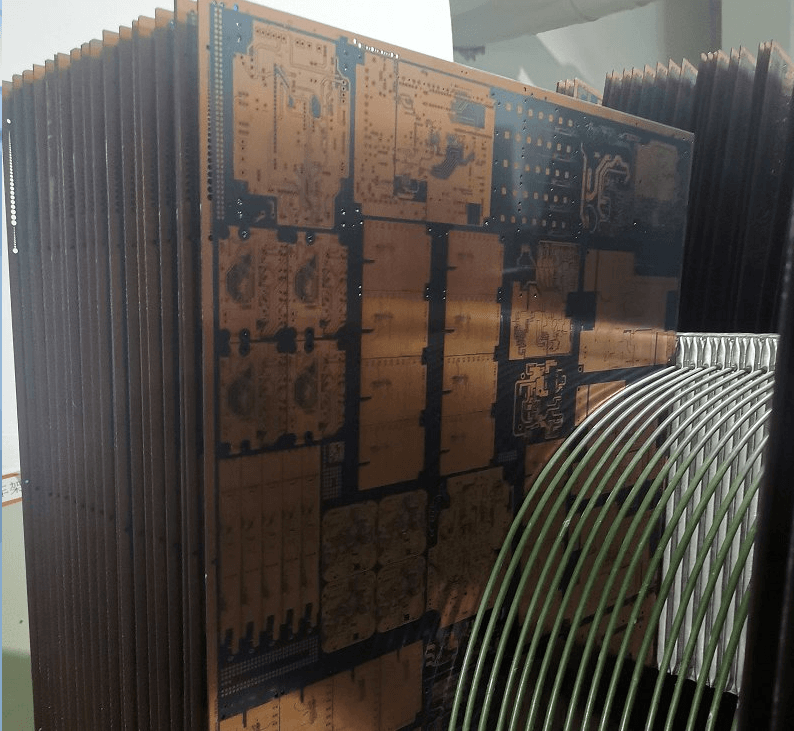
As shown in the figure above, the design draft of the PCB is finally assembled on a large working panel for production. For characteristic impedance control, the uniformity of the resin flow during the lamination of the entire large panel cannot be ignored. The performance of the lamination equipment used at this time will be crucial.
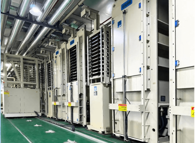
Equipment is one of the important factors affecting the quality of high-layer boards. To this end, Jiali Chuang uses first-class equipment in the industry to produce high-layer boards to ensure product quality.
Lamination machine
After laminating, it comes to the drilling process, followed by the same process flow as single- and double-sided boards, but there are also some differences. For example, Jiali Chuang has launched a free service to improve PCB quality for the manufacture of high-layer boards.
One is the improved immersion gold process.
Immersion gold is a relatively expensive surface treatment method in the industry, which can provide good electrical connection, corrosion resistance and welding performance. The immersion gold layer can provide a smooth and uniform metal surface, which helps to maintain good signal transmission and impedance control. In addition, it can ensure the stability and durability of the metal layer during the welding process, provide excellent corrosion resistance, and extend the service life of the PCB. In addition to the immersion gold process, Jiali Chuang uses the plate-in-hole process (resin plug hole + electroplating cap) for 6-32 layer boards for free. Vias are very important for the quality of PCBs because they play an important role in electronic devices, supporting the realization of complex circuits and the reliability of functions. Due to various factors, the vias will be corroded slowly, resulting in connection failure, signal attenuation, short circuit and leakage, and reliability problems, while the via-in-disk process effectively solves these problems.
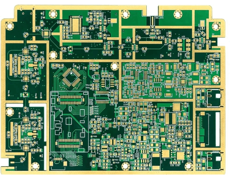
PCB produced by immersion gold process and via-in-disk process
In short, the manufacturing of multi-layer boards is not as simple as adding an inner layer process compared to single- and double-sided boards, nor is it just throwing the PCB production draft directly to the PCB board factory. At least in the PCB design link, we should understand the process capabilities of the PCB board factory and introduce DFM for manufacturability design during design. Before actually implementing wiring, we need to communicate with the PCB board factory to determine the required board and stacking structure to meet the performance requirements of the specific transmission line structure and be able to manufacture at a reasonable cost and time.