Manufacturing process of multilayer pcb
Overview Of Multilayer PCB Manufacturing Process
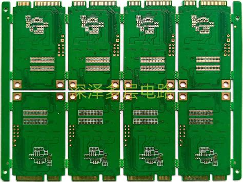
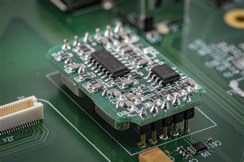
The manufacturing process of multilayer printed circuit boards (PCBs) is a complex and intricate procedure that requires precision and attention to detail. Multilayer PCBs are essential components in modern electronic devices, offering enhanced functionality and compactness by integrating multiple layers of circuitry within a single board. The process begins with the design phase, where engineers use specialized software to create a detailed blueprint of the PCB layout. This design includes the arrangement of various electronic components and the interconnections between them, ensuring optimal performance and reliability.
Once the design is finalized, the manufacturing process moves to the fabrication stage.
This involves the creation of individual layers that will eventually be stacked to form the multilayer PCB. Each layer is made from a thin sheet of insulating material, typically fiberglass-reinforced epoxy resin, known as the substrate. Copper foil is laminated onto the substrate to form the conductive pathways. The copper is then etched away using a chemical process to leave behind the desired circuit pattern. This etching process is repeated for each layer, with extreme precision required to ensure that the circuits align perfectly when the layers are stacked.
Following the fabrication of individual layers, the next step is the lamination process.
During lamination, the layers are carefully aligned and bonded together under high temperature and pressure. This step is crucial, as any misalignment can lead to circuit failures or reduced performance. The lamination process not only fuses the layers into a single, cohesive unit but also ensures the mechanical stability and durability of the PCB. After lamination, the board undergoes drilling to create holes for the placement of electronic components and for vias, which are conductive pathways that connect different layers of the PCB.
Subsequently, the drilled holes are plated with copper to establish electrical connections between the layers.
This plating process involves depositing a thin layer of copper onto the walls of the holes, ensuring that the electrical signals can travel seamlessly through the board. Once the plating is complete, the PCB undergoes a series of tests to verify its electrical integrity and functionality. These tests are critical to identify any defects or issues that may have arisen during the manufacturing process.
After successful testing, the PCB is ready for the solder mask application.
The solder mask is a protective layer applied to the surface of the PCB to prevent solder bridges and protect the copper traces from environmental damage. It also provides insulation and enhances the board’s overall appearance. The final step in the manufacturing process is the application of a silkscreen layer, which involves printing labels, component identifiers, and other markings onto the PCB. This layer aids in the assembly and maintenance of the board by providing clear visual guidance.
In conclusion, the manufacturing process of multilayer PCBs is a meticulous and highly technical endeavor that requires a combination of advanced technology and skilled craftsmanship. From the initial design to the final testing and finishing touches, each step is crucial in ensuring the production of high-quality PCBs that meet the demanding requirements of modern electronic devices. As technology continues to evolve, the manufacturing processes for multilayer PCBs will undoubtedly advance, further enhancing their capabilities and applications in various industries.
Key Steps In Multilayer PCB Lamination
The manufacturing process of multilayer printed circuit boards (PCBs) is a complex and intricate procedure that requires precision and attention to detail. At the heart of this process lies the lamination of multiple layers, which is crucial for the functionality and reliability of the final product. Understanding the key steps involved in multilayer PCB lamination is essential for anyone involved in electronics manufacturing or design.
Initially, the process begins with the preparation of individual layers, which are typically composed of a substrate material such as fiberglass-reinforced epoxy resin, known as FR-4.
Each layer is meticulously etched with the desired circuit pattern using a photolithographic process. This involves coating the substrate with a photosensitive material, exposing it to ultraviolet light through a mask, and then developing the image to reveal the circuit pattern. Once the etching is complete, the layers are thoroughly cleaned to remove any residual chemicals or debris.
Following the preparation of individual layers, the next step involves aligning and stacking them in the correct sequence.
This alignment is critical, as any misalignment can lead to electrical failures or short circuits in the final product. To ensure precision, manufacturers often use optical alignment systems that can detect even the slightest deviations. Once aligned, the layers are temporarily held together using a tacky adhesive, which allows for minor adjustments before the final lamination.
The lamination process itself is a delicate balance of heat, pressure, and time.
The stacked layers are placed in a lamination press, where they are subjected to high temperatures and pressures. This causes the adhesive to flow and bond the layers together, creating a single, cohesive unit. The temperature and pressure must be carefully controlled to prevent defects such as delamination or voids, which can compromise the integrity of the PCB. Typically, the lamination cycle lasts several hours, during which the layers are gradually heated and then cooled to ensure a strong bond.
Once the lamination is complete, the newly formed multilayer PCB undergoes a series of inspections and tests to verify its quality and functionality.
These inspections often include visual checks for surface defects, as well as electrical tests to ensure that the circuits are properly connected and functioning as intended. Any defects identified at this stage can often be traced back to issues during the lamination process, highlighting the importance of precision and control throughout the procedure.
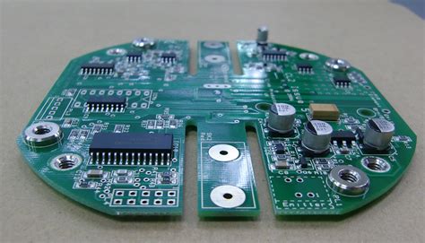
After passing inspection, the multilayer PCB is ready for further processing, which may include drilling holes for component leads, plating through-holes to establish electrical connections between layers, and applying a solder mask to protect the circuits from environmental damage. Each of these steps builds upon the foundation established during the lamination process, underscoring its critical role in the overall manufacturing of multilayer PCBs.
In conclusion, the lamination of multilayer PCBs is a vital step in their manufacturing, requiring careful preparation, precise alignment, and controlled application of heat and pressure. By understanding and mastering these key steps, manufacturers can produce reliable and high-quality PCBs that meet the demands of modern electronic devices. As technology continues to advance, the importance of meticulous lamination processes will only grow, ensuring that multilayer PCBs remain at the forefront of electronic innovation.
Challenges In Multilayer PCB Fabrication
The manufacturing process of multilayer printed circuit boards (PCBs) is a complex and intricate endeavor, presenting numerous challenges that require careful consideration and precise execution. As the demand for more compact and efficient electronic devices continues to grow, the need for multilayer PCBs has become increasingly prevalent. These PCBs, which consist of multiple layers of conductive material separated by insulating layers, offer enhanced functionality and performance. However, the fabrication of such sophisticated components is fraught with challenges that manufacturers must navigate to ensure quality and reliability.
One of the primary challenges in multilayer PCB fabrication is the precise alignment of the various layers.
Each layer must be meticulously aligned to ensure that the electrical connections between them are accurate and reliable. Misalignment can lead to short circuits, open circuits, or other defects that compromise the functionality of the final product. To address this issue, manufacturers employ advanced alignment techniques and equipment, such as optical alignment systems, to achieve the necessary precision. Despite these technological advancements, maintaining alignment remains a critical challenge, particularly as the number of layers increases.
In addition to alignment, the lamination process poses significant challenges in multilayer PCB fabrication.
During lamination, the individual layers are bonded together under heat and pressure to form a single, cohesive unit. This process must be carefully controlled to prevent defects such as delamination, where layers separate, or voids, which are air pockets trapped between layers. These defects can severely impact the electrical performance and structural integrity of the PCB. Manufacturers must carefully select materials and optimize process parameters, such as temperature and pressure, to minimize the risk of such defects.
Another challenge is the drilling process, which involves creating holes, or vias, that allow electrical connections between layers.
The precision required in drilling is paramount, as any deviation can result in misalignment or damage to the conductive pathways. The use of advanced drilling technologies, such as laser drilling, has improved accuracy, but the process remains challenging, especially for PCBs with a high density of vias. Furthermore, the aspect ratio, which is the ratio of the hole depth to its diameter, becomes a critical factor in ensuring reliable connections, particularly in thicker multilayer PCBs.
Moreover, the etching process, which removes excess copper to create the desired circuit patterns, presents its own set of challenges.
Achieving uniform etching across all layers is essential to maintain the integrity of the circuit design. Variations in etching can lead to inconsistencies in trace width and spacing, potentially causing electrical failures. Manufacturers must carefully control the etching process, often employing advanced chemical solutions and equipment to achieve the necessary precision.
Finally, testing and quality assurance are crucial steps in the fabrication of multilayer PCBs.
Given the complexity of these components, thorough testing is essential to identify any defects or issues before the PCBs are integrated into electronic devices. Manufacturers employ a range of testing methods, including electrical testing and X-ray inspection, to ensure that each PCB meets the required specifications. Despite these efforts, the intricate nature of multilayer PCBs means that achieving 100% defect-free production remains a significant challenge.
In conclusion, the fabrication of multilayer PCBs involves navigating a series of complex challenges, from precise alignment and lamination to drilling, etching, and testing. Each step requires meticulous attention to detail and advanced technological solutions to ensure the production of high-quality, reliable PCBs. As technology continues to evolve, manufacturers must continually adapt and innovate to overcome these challenges and meet the growing demands of the electronics industry.
Innovations In Multilayer PCB Production Techniques
The manufacturing process of multilayer printed circuit boards (PCBs) has undergone significant innovations, driven by the increasing demand for compact, efficient, and high-performance electronic devices. As technology advances, the need for more complex and densely packed PCBs has become paramount, leading to the development of sophisticated production techniques. These innovations not only enhance the functionality of electronic devices but also improve the efficiency and reliability of the manufacturing process itself.
To begin with, the production of multilayer PCBs involves several intricate steps, each of which has been refined through technological advancements.
Initially, the process starts with the design phase, where computer-aided design (CAD) software is employed to create precise layouts of the circuit. This digital blueprint is crucial as it dictates the subsequent steps in the manufacturing process. Once the design is finalized, the focus shifts to the preparation of the substrate material, typically a fiberglass-reinforced epoxy laminate, which serves as the foundation for the PCB.
Following the preparation of the substrate, the next step involves the application of a conductive material, usually copper, onto the substrate.
This is achieved through a process known as lamination, where multiple layers of copper and substrate are bonded together under heat and pressure. Recent innovations in lamination techniques have introduced advanced materials and processes that enhance the thermal and electrical properties of the PCB, thereby improving its overall performance.
Subsequently, the laminated board undergoes a series of etching processes to remove excess copper and define the circuit patterns.
Innovations in etching technology, such as laser etching, have allowed for greater precision and reduced material wastage, contributing to more efficient production. Moreover, these advancements have enabled the creation of finer circuit lines, which are essential for the miniaturization of electronic components.
Once the circuit patterns are established, the focus shifts to the drilling process, where holes are created to connect the different layers of the PCB.
Traditional mechanical drilling has been largely supplemented by laser drilling techniques, which offer higher accuracy and the ability to create smaller vias. This is particularly important in multilayer PCBs, where space is at a premium and the interconnection of layers is critical for functionality.
After drilling, the PCBs undergo a plating process to coat the holes and circuit paths with a conductive material, typically copper.
This step ensures electrical connectivity between the layers. Innovations in plating techniques, such as the use of electroless plating, have improved the uniformity and adhesion of the conductive coating, thereby enhancing the reliability of the PCB.
Finally, the PCBs are subjected to a series of testing and inspection procedures to ensure they meet the required specifications and quality standards.
Automated optical inspection (AOI) and X-ray inspection are among the advanced techniques employed to detect any defects or inconsistencies in the PCBs. These innovations have significantly reduced the likelihood of faulty products reaching the market, thereby increasing consumer confidence in electronic devices.
In conclusion, the manufacturing process of multilayer PCBs has been revolutionized by a series of innovations that have improved both the efficiency and quality of production. From advanced design software to cutting-edge etching and drilling techniques, each step in the process has been optimized to meet the growing demands of modern electronics. As technology continues to evolve, it is likely that further advancements will continue to shape the future of multilayer PCB production, driving the development of even more sophisticated electronic devices.