Mastering Complex PCB Assembly: Techniques for Success
Key Takeaways
Mastering complex PCB assembly (often referred to as PCBA) is not just about following a set of instructions; it necessitates a deep understanding of several fundamental principles. A solid grasp of PCB design principles is crucial as it lays the groundwork for successful assembly. Each layer of a multi-layer PCB presents unique challenges, thus careful planning in component placement becomes vital to ensure performance and reliability. Moreover, the integration of advanced soldering techniques can significantly enhance joint integrity, particularly in densely packed assemblies where precision is paramount. As manufacturers navigate the complexities intrinsic to multi-layer designs, adopting stringent quality control methods is indispensable. These practices not only ensure that each assembly meets the required standards but also bolster efficiency across production lines. In this competitive landscape, embracing emerging technologies within PCB assembly processes can further streamline operations and reduce costs while maintaining high quality. By following these key takeaways, professionals can enhance their proficiency in PCBA and contribute to creating dependable electronic devices that meet the demands of modern technology.
Understanding PCB Design Principles
Mastering PCB assembly requires a solid foundation in PCB design principles. A well-designed PCBA serves as the cornerstone for any successful electronics project, influencing both functionality and manufacturability. Understanding the basic concepts such as circuit layout, signal integrity, and electrical characteristics can significantly impact the performance of the final product.
A thorough grasp of the design rules is essential. For instance, maintaining appropriate spacing between traces prevents electrical interference and enhances reliability. Moreover, the choice of materials—such as the substrate or copper thickness—can affect thermal performance and signal speed. Designers must also consider design for manufacturability (DFM) to ensure that their boards can be efficiently produced without compromising quality.
| Design Considerations | Description |
|---|---|
| Trace Width & Spacing | Ensures adequate current-carrying capacity and minimizes crosstalk |
| Via Sizes | Impacts assembly process and space utilization |
| Layer Stack-up | Determines signal routing efficiency and EMI considerations |
In addition to technical specifications, it’s important to incorporate flexibility in the design to accommodate potential changes or updates in technology. The integration of simulation tools can provide valuable pre-assembly testing insights that highlight potential issues before they arise during actual PCB assembly.
“Effective PCB design not only focuses on current needs but anticipates future enhancements.”
This proactive approach to design can minimize disruptions during the PCBA process, ultimately leading to greater efficiency in manufacturing while ensuring that quality remains paramount throughout production cycles. Emphasizing precision in your design methodology can significantly contribute to achieving a successful assembly outcome.
Key Considerations for Component Placement
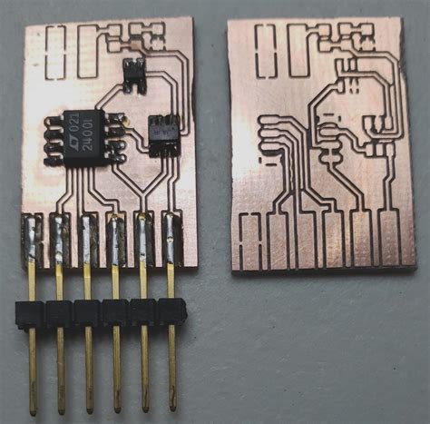
When it comes to pcb assembly, one of the most critical aspects is the strategic component placement. This process not only affects the aesthetic layout of the printed circuit board but also plays a significant role in the overall performance and reliability of the final product. Efficient component placement must take into account factors such as signal integrity, thermal management, and ease of soldering. For instance, placing sensitive components away from high-frequency paths can help prevent interference, ensuring optimal performance in pcba applications.
In addition, designers should consider the physical size and orientation of components to facilitate easier soldering processes later in the assembly line. Grouping similar components can also streamline manufacturing, making it easier to manage processes like solder paste application and inspection. Furthermore, implementing a PCB layout that minimizes trace lengths contributes to reducing potential latency issues, which is essential for maintaining high signal integrity.
Lastly, employing advanced software tools for conducting simulations can provide invaluable insights into potential issues that may arise during assembly. By prioritizing thoughtful and deliberate component placement, manufacturers can significantly enhance their production efficiency and durability of products in the competitive landscape of electronic manufacturing. The synergy between careful planning during design and effective execution during assembly will ultimately lead to higher quality pcb assembly outcomes and more reliable end products.

Advanced Soldering Techniques for Complex Assemblies
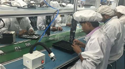
When it comes to pcb assembly, especially in more intricate designs, advanced soldering techniques play a pivotal role in ensuring reliable connections and enhanced performance of the final product. One effective method that has gained prominence is surface mount technology (SMT), which allows for the placement of components directly onto the surface of the printed circuit board. This technique not only facilitates efficient use of space but fosters a significant reduction in assembly time, which is crucial for high-volume production. Additionally, employing techniques such as reflow soldering and wave soldering can help streamline the process, as these methods allow for uniform heating and consistent solder joint quality across various component types. Understanding thermal management during these processes is also essential; it ensures that components are not exposed to excessive heat, which could potentially damage sensitive parts or lead to performance failures. Implementing these techniques during the pcba process promotes an increase in overall operational reliability, thus setting a strong foundation for successful electronic manufacturing outcomes.
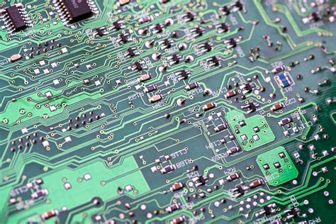
Managing Challenges in Multi-layer PCB Assembly
Managing challenges in multi-layer PCB assembly (PCBA) involves a thorough understanding of both the design complexities and the operational aspects of assembling printed circuit boards. One of the primary hurdles is ensuring proper alignment and registration during the assembly process. With multiple layers, maintaining precision in component placement is crucial; even a slight misalignment can lead to significant performance issues. Furthermore, advanced soldering techniques must be utilized to accommodate various layers and materials, ensuring strong connections without compromising component integrity or performance.
Another vital consideration is thermal management; as multiple layers can generate increased heat, careful design and assembly techniques must mitigate this risk. The integration of high-density interconnects can also pose a challenge, requiring specialized tools and methodologies to ensure reliable connections throughout the stack-up. Additionally, adherence to strict quality control measures during PCB assembly not only enhances reliability but also minimizes potential defects that could arise from layer-to-layer interactions.
In essence, successfully navigating these challenges necessitates an in-depth knowledge of both electrical and mechanical properties inherent within multi-layer PCBA constructs, alongside implementing industry best practices and leveraging emerging technologies that promote efficiency and reliability throughout the process. By addressing these complexities head-on, manufacturers can achieve a higher standard of excellence in their products while ensuring that customer satisfaction remains paramount.
Quality Control Methods in PCB Manufacturing
Ensuring the highest standards in PCB assembly requires a robust quality control (QC) framework. The QC process begins with the careful examination of design files to confirm that the layout adheres to established industry standards and guidelines. Employing automated Optical Inspection (AOI) systems is crucial for identifying defects such as misplaced components or soldering issues, which can compromise the integrity of the PCBA. Additionally, implementing in-circuit testing (ICT) allows for assessing the functionality of individual components within the assembled PCB, ensuring they operate correctly before final inspection.
Moreover, maintaining a clean and controlled manufacturing environment plays a vital role in preventing contaminants that may affect solder joints and overall board reliability. Regular training sessions for staff on best practices and emerging QC technologies foster a culture of excellence in pcb assembly processes. Ultimately, a comprehensive QC strategy not only enhances the product’s reliability but also builds customer trust by ensuring high-quality output in every stage of PCB manufacturing.
Optimizing Workflow for Enhanced Efficiency
In the realm of PCB assembly (pcba), achieving an optimized workflow is crucial for enhancing overall efficiency and reliability. Streamlining the assembly process involves several strategies that focus on both time and resource management. First, adopting a well-organized workstation layout can significantly reduce unnecessary movements and minimize the risk of component misplacement. This includes clearly labeling tools and components assigned to specific tasks, enabling swift access when needed. Additionally, implementing a robust just-in-time inventory system can prevent excess stock while ensuring that essential components are readily available when required. This approach not only lowers costs but also instills flexibility into the pcb assembly process.
Moreover, utilizing modern software tools for project management assists teams in tracking progress, setting timelines, and managing deadlines effectively. These systems often support real-time updates, which foster better communication among team members and drive collaborative efforts towards overcoming potential challenges in complex pcba projects. As technology evolves, incorporating automation into repetitive tasks can lead to enhanced precision and speed in soldering and component placement, reducing the potential for human error.
Finally, regularly assessing workflow performance is essential. Gathering feedback from team members can unveil bottlenecks that may not be immediately apparent and encourage continuous improvement initiatives aimed at refining processes within complex PCB assembly environments. Emphasizing these aspects will undoubtedly lead to a more efficient workflow, ensuring high-quality outputs while meeting stringent production demands.
Emerging Technologies in PCB Assembly
The landscape of PCB assembly (pcba) is continuously evolving, driven by emerging technologies that enhance precision, efficiency, and scalability. Among these advancements, automated assembly processes stand out, significantly reducing labor costs and minimizing errors. Techniques such as surface mount technology (SMT) have transformed the way components are placed on printed circuit boards, allowing for tighter packing and improved performance. Additionally, the incorporation of robotics in assembly lines has streamlined the handling of intricate components, ensuring consistent quality and reliability in the final product. Another promising area is the integration of Internet of Things (IoT) devices within assembly equipment, which facilitates real-time monitoring and data analytics. This capability allows manufacturers to anticipate issues before they arise, leading to enhanced reliability throughout the pcb assembly process. Furthermore, advancements in material science have led to the development of more robust substrates that are not only lightweight but also capable of handling higher thermal loads—a crucial factor as electronic devices become increasingly compact and powerful. These innovations collectively represent a pivotal shift in how pcba processes are approached, setting new standards for quality and efficiency in electronics manufacturing.
Best Practices for Testing and Validation
Testing and validation are critical phases in the pcb assembly process, ensuring that the final product meets design specifications and operational requirements. The complexity of pcba, particularly in multi-layer designs, necessitates a comprehensive testing strategy that encompasses both functional and structural assessments. It’s essential to begin with in-circuit testing (ICT), which allows for early detection of potential faults by verifying connections and component functionality before assembly is finalized. Following this, employing automated optical inspection (AOI) can catch visual defects such as solder bridges or misalignment, enhancing overall quality control.
Additionally, it’s important to establish a robust validation procedure that includes environmental testing to assess the board’s performance under various conditions. This can range from temperature cycling to humidity exposure tests, ensuring that the pcb assembly can withstand real-world applications. Implementing thorough burn-in tests also helps identify any latent defects by exposing the assembly to elevated stress conditions for a specified duration.
Moreover, incorporating feedback loops into your testing processes facilitates continuous improvement. Data collected during testing can inform design modifications for future iterations of pcba, thus optimizing performance and reliability. By ensuring stringent evaluation protocols at every stage of assembly, manufacturers can significantly mitigate risks associated with complex pcb assemblies, leading to increased customer satisfaction and minimized returns due to failures.
Conclusion
In the realm of PCB assembly, achieving success in complex projects requires a well-rounded understanding of various integral components of the process. Mastering pcba not only relies on following established design principles but also on implementing proven techniques that streamline operations and ensure optimal outcomes. Throughout this article, we have delved into essential aspects such as component placement, which is crucial in preventing errors and enhancing functionality, as well as advanced soldering techniques that bolster reliability in pcb assembly. As we continue to push the boundaries of technology, embracing emerging trends and refining our approaches will remain vital. Whether dealing with multi-layer boards or navigating challenges specific to intricate designs, adhering to established best practices will lead to improved quality control and a more efficient workflow. Ultimately, a commitment to continuous improvement in both processes and technologies will enable manufacturers to excel in pcba, driving innovation forward in electronics manufacturing.
FAQs
What is complex PCB assembly?
Complex PCB assembly, or PCBA, refers to the process of integrating various electronic components onto a printed circuit board with intricate designs, often involving multiple layers and advanced technology.
What are the key considerations for successful component placement in PCB assembly?
When placing components on a board, consider factors such as electrical performance, thermal management, and the accessibility of each component for future maintenance or replacement. Proper planning can significantly enhance the overall efficiency of the pcb assembly process.
What advanced soldering techniques should be used in complex PCBs?
Techniques like reflow soldering, wave soldering, and selective soldering are essential for achieving reliable connections in complex assemblies. Each method has its specific applications and benefits that contribute to the durability of the PCBA.
How can challenges in multi-layer PCB assembly be managed?
Effective management involves meticulous planning to ensure correct layer alignment, as well as robust quality checks throughout the production process. Utilizing simulation software can also help identify potential issues before actual manufacturing begins.
What quality control methods are employed in PCB manufacturing?
Quality control may include visual inspections, automated optical inspection (AOI), and functional testing processes to ensure that each unit meets stringent performance standards before delivery.
How can workflow be optimized for enhanced efficiency in PCB assembly?
Streamlining processes by adopting lean manufacturing principles and ensuring proper training for staff can greatly improve productivity. Transitioning to more automated systems may also reduce human error and increase output rates.
What emerging technologies are impacting PCB assembly?
Technologies such as additive manufacturing, artificial intelligence, and IoT integration are transforming how pcb assembly is performed, making it possible to achieve higher accuracy and faster production times.
For more information on enhancing your PCB assembly, please visit our page here: AndwinPCB – PCB Assembly


