Mastering Creation: A Comprehensive Guide to PCB Assembly
Key Takeaways
In mastering the process of PCB assembly, several critical components come into play that can greatly influence the outcome of your project. First and foremost, a solid foundation in the basics of PCB design is essential. This knowledge enables designers and engineers to create efficient layouts that minimize interference and optimize signal integrity. Additionally, familiarity with essential tools and software used in PCBA can enhance productivity and streamline workflows.
Understanding the step-by-step process involved in PCB creation allows for a more systematic approach, ensuring no aspect is overlooked during assembly. Careful consideration must also be given to component placement and soldering techniques, as these are key factors in achieving high-quality connections and functionality. Familiarity with common challenges faced during PCB assembly, such as thermal issues or alignment errors, empowers one to implement effective solutions proactively.
Moreover, implementing rigorous quality control measures throughout production will help maintain high standards. Continually exploring advanced techniques for optimizing performance not only improves the reliability of your boards but also keeps your designs competitive. Finally, staying informed about future trends in PCB technology ensures that your skills remain relevant in an ever-evolving field. By integrating these takeaways into practice, you can develop a thorough understanding of PCBA that encompasses both foundational knowledge and innovative developments.
Understanding the Basics of PCB Design
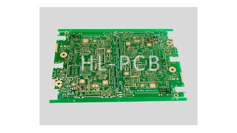
When it comes to PCB assembly, understanding the foundational elements of PCB design is crucial for achieving successful results in the creation process. A printed circuit board (PCB) is the backbone of electronic devices, providing both mechanical support and electrical pathways for components like resistors, capacitors, and integrated circuits. The first step involves defining the schematic layout, which serves as a blueprint for the electrical connections. Employing tools such as Eagle, Altium Designer, or KiCAD, designers can create detailed schematics that translate into PCB layouts.
It’s essential to consider factors such as layer count, material type, and trace width when designing a PCB. For instance, multi-layer boards enable more complex designs but also increase production costs and complexity in PCBA processes. Additionally, maintaining sufficient spacing between traces is vital to minimize interference and ensure reliability.
| Design Factor | Importance |
|---|---|
| Layer Count | Determines complexity and functionality of design |
| Material Type | Affects conductivity and durability |
| Trace Width | Influences current carrying capacity |
“A well-planned PCB design can save you from countless headaches during assembly.”
Moreover, adhering to industry best practices during the design phase can simplify the subsequent steps in PCB assembly. Consider implementing design rule checks (DRC) early in the process to identify potential issues before moving on to production. This proactive approach not only enhances efficiency but also plays a pivotal role in ensuring high-quality outcomes in electronic circuit board development.
In conclusion, mastering the basics of PCB design is a vital component of successful pcba processes. By prioritizing effective designs and employing suitable tools, both newcomers and seasoned professionals can elevate their understanding and execution of PCB projects significantly.
Essential Tools and Software for PCB Assembly
When embarking on the journey of PCB assembly, having the right tools and software is crucial for ensuring efficiency and quality in the creation process. At the foundational level, basic tools such as soldering irons, multimeters, and PCB holders are essential. These devices facilitate precise work during assembly, allowing for accurate connections and troubleshooting. In terms of software, design programs like Altium Designer or Eagle are pivotal in creating and simulating circuit layouts before they are physically assembled. These tools not only help in visualizing the layout but also assist with checking electrical integrity, which is vital for reliable performance.
Moreover, specialized applications for PCBA processes can significantly streamline workflows. Software solutions that offer capabilities like component libraries, automated design rule checks, and realistic simulations foster a smoother transition from prototype to production. Additionally, tools that cater to collaboration among team members can enhance communication, ultimately leading to a more polished final product. By combining skilled tooling with advanced software options, creators can achieve optimum results in their PCB assembly endeavors, ensuring high-quality electronic circuit boards that meet both functionality and durability standards.
Step-by-Step Guide to the PCB Creation Process
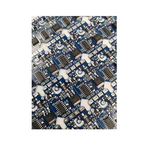
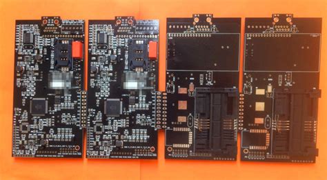
The process of PCB assembly or PCBA is a nuanced journey, requiring careful planning and execution. It begins with the creation of a PCB design, which is crucial as it lays the foundation for the entire assembly process. This stage typically involves using specialized software to create a schematic that defines how components are interconnected. Once the design is complete, the next step involves converting it into a physical board using techniques like etching and layering. After this, components are placed on the board according to the layout, ensuring that each is positioned correctly for optimal performance.
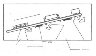
Following placement, soldering becomes vital. This can be performed manually or through automated processes such as reflow or wave soldering, which require precision to prevent defects. As you move forward in this step-by-step journey, maintaining focus on techniques like thermal management and ensuring appropriate clearances between components will be beneficial.
Once soldering is complete, inspection and testing are paramount. Implementing techniques such as visual inspection, automated optical inspection (AOI), or functional testing can help identify any faults early in the production process. Addressing any discrepancies promptly can significantly enhance the overall quality of your PCB assembly.
In summary, mastering each phase of the PCB creation process—from design through inspection—ensures that your final product meets both functional standards and quality expectations in this ever-evolving field of electronics.
Best Practices for Component Placement and Soldering
In pcb assembly, the effective placement of components is critical to the overall performance and reliability of the final product. Proper component placement involves understanding the circuit design and strategically positioning components to minimize noise, optimize signal paths, and facilitate heat dissipation. It is advisable to group similar components together, such as capacitors and resistors, to streamline connections and improve manufacturing efficiency. When dealing with pcba, ensure that tolerance levels are respected; components should not be too close to each other as this can lead to solder bridging or increased thermal issues.
During the soldering process, it’s crucial to use the right techniques and tools to ensure strong connections. Techniques such as reflow soldering or wave soldering should be employed based on the component types and layout complexities. Additionally, proper temperature control is essential to avoid damage during soldering; an appropriate heating profile can prevent issues like thermal shock or insufficient thermal transfer.
Maintaining a clean work environment will also enhance the quality of solder joints. Contaminants such as dust or grease can cause weak connections or poor conductivity; therefore, always handle components with clean tools and ensure that surfaces are free of impurities before proceeding with soldering. By adhering to these best practices in component placement and soldering during pcb assembly, manufacturers can achieve higher-quality results, leading to more reliable electronic devices that perform effectively in their intended applications.
Common Challenges in PCB Assembly and Solutions
PCB assembly, often abbreviated as PCBA, is a complex process that can present various challenges. One common challenge is ensuring proper component placement. Misalignment can lead to poor electrical connections or, in some cases, complete circuit failure. To mitigate this issue, meticulous attention to the design stage is critical; utilizing accurate design tools and thorough verification processes can help catch potential placement issues early. Another frequent hurdle is soldering defects such as cold joints or bridging. These problems typically arise from inadequate heat application or excessive solder material. Adopting best practices such as consistent temperature control and employing automated soldering techniques can significantly enhance solder quality.
Additionally, variances in component quality can lead to inconsistencies in the performance of the assembled PCB. This emphasizes the importance of sourcing components from reputable suppliers and implementing stringent quality checks before commencing the assembly process. Environmental factors during assembly also pose challenges—humidity levels, for instance, can affect the reliability of solder and components alike. Maintaining controlled assembly environments will ensure optimal conditions for pcba.
Lastly, communication breakdowns between design and manufacturing teams can result in delays or errors in production. Establishing efficient workflows that promote collaboration ensures that everyone involved has a clear understanding of expectations and requirements, ultimately paving the way for a smoother PCB assembly process. Addressing these challenges with strategic solutions not only improves efficiency but ensures the creation of high-quality electronic circuit boards essential for today’s technology-driven landscape.
Quality Control Measures in PCB Production
Ensuring high standards in PCB assembly is critical for the reliability and performance of electronic devices. Quality control measures begin at the design phase, where adherence to established design rules can mitigate potential issues during the assembly process. Utilizing automated optical inspection (AOI) systems significantly enhances quality assurance, detecting defects such as misaligned components or insufficient solder joints before they emerge as larger issues.
Moreover, implementing rigorous testing protocols during various stages of the PCBA process is essential. Functional testing, for example, checks if the assembled circuit board performs to specifications under various conditions, while in-circuit testing can identify problems at the component level. This process ensures that each PCB assembly meets defined criteria for both functionality and durability.
To further enhance quality control, embracing a culture of continuous improvement among team members fosters an environment where everyone plays a role in monitoring and improving processes. Utilizing statistical process control (SPC) techniques allows manufacturers to analyze production data in real-time, ensuring that any deviations from the norm are addressed promptly.
Additionally, thorough documentation and traceability throughout the PCBA lifecycle are vital not only for quality assurance but also for regulatory compliance. By maintaining detailed records of materials used, assembly processes, and test results, manufacturers can swiftly pinpoint problems should they arise post-production.
In summary, robust quality control measures are indispensable in PCB production. They not only prevent defects but also ensure that each PCB assembly is a reliable component of any electronic system.
Advanced Techniques for Optimizing Performance
When it comes to pcb assembly, integrating advanced techniques is essential for enhancing overall performance and efficiency. One pivotal strategy involves utilizing high-frequency design techniques, which ensure that the pcba can handle faster signal transitions without degrading performance. Additionally, implementing smaller trace widths and via sizes not only maximizes space but also improves signal integrity by reducing parasitic capacitance and inductance.
Thermal management plays a crucial role in pcb assembly as well, particularly in high-power applications. Techniques such as thermal vias and copper pours can effectively dissipate heat and maintain optimal working temperatures for components, minimizing the risk of thermal failure. Furthermore, careful consideration of component placement during the initial design phase significantly contributes to optimizing performance; placing heat-sensitive components away from heat-generating ones is a best practice that aids in maintaining device longevity.
Finally, embracing innovative materials like low-loss substrates can significantly improve the performance of pcba by reducing signal loss over distance, allowing for clearer transmission of data. By incorporating these advanced techniques into the pcb assembly process, designers and manufacturers alike can ensure that their electronic devices perform at peak efficiency while meeting the ever-evolving demands of modern technology.
Future Trends in PCB Technology and Assembly
As industries continue to evolve, so too does PCB assembly technology, with several key trends shaping the future of PCBA processes. One significant advancement is the increasing integration of automated manufacturing systems, which harness robotics and artificial intelligence to streamline assembly lines, reduce human error, and enhance precision. This evolution not only speeds up production but also allows for the rapid adaptation of pcb assembly techniques in response to changing market demands. Additionally, there is a growing emphasis on sustainability, with manufacturers exploring eco-friendly materials and practices aimed at reducing waste and energy consumption in the PCB assembly process. Another notable trend is the rise of miniaturization, pushing engineers to create smaller, more efficient circuit boards without compromising functionality or performance. This trend encourages innovations in both design and manufacturing processes, leading to more compact electronic devices that meet consumer demands for portability. Finally, the future of PCBA also points toward enhanced connectivity and functionality through advances in smart technology, enabling increasingly sophisticated electronics that interact seamlessly with our daily lives. As these trends continue to develop, staying informed on the latest innovations will be essential for both professionals and enthusiasts involved in PCB assembly.
Conclusion
In summary, mastering the intricacies of PCB assembly (or PCBA) is crucial for anyone involved in electronics design and production. The journey from initial design to final assembly involves a series of well-defined processes that not only require technical expertise but also a keen understanding of best practices. As you explore the world of PCB assembly, it’s essential to grasp the fundamental concepts, including layout optimization and effective component placement. Overcoming common challenges such as soldering issues or component misalignment is part of perfecting this craft. Additionally, implementing quality control measures can significantly elevate your production standards, ensuring that every board meets the required specifications. Keeping abreast of future trends in PCB technology will also help you stay competitive in a rapidly evolving market. By continually refining your skills and embracing innovative techniques, you can greatly enhance your proficiency in the creation and assembly of electronic circuit boards, establishing a strong foundation for success in any project involving PCBA.
FAQs
What is PCB assembly?
PCB assembly, often abbreviated as PCBA, refers to the process of soldering electronic components onto a printed circuit board. This crucial step transforms a bare board into a functional electronic device.
What materials are used in PCB assembly?
The primary materials used in pcb assembly include copper-clad laminates, solder paste, and various electronic components such as resistors, capacitors, and integrated circuits. These materials ensure reliable electrical connections and optimal performance.
What are the common methods of soldering in PCB assembly?
The most common soldering methods in pcba include reflow soldering, wave soldering, and hand soldering. Each method has its advantages and is chosen based on production volume and design complexity.
How can I ensure high-quality PCB assembly?
To guarantee high-quality pcb assembly, it’s essential to implement rigorous quality control measures throughout the assembly process, including thorough inspections, testing for connectivity, and verifying component placements.
What challenges are faced during PCB assembly?
Common challenges include component misalignment, cold solder joints, and the presence of contaminants. Familiarity with best practices can help mitigate these issues effectively.
For More Information
For an in-depth insight into PCB assembly procedures and optimization techniques, please click here.