Mastering Double Sided PCB Assembly for Optimal Performance
Key Takeaways
Understanding the intricacies of double sided PCB assembly is crucial for anyone looking to achieve optimal performance in their electronic projects. When it comes to pcb assembly, familiarity with fundamental concepts enables designers to create layouts that maximize space and functionality. Effective layout design should consider the unique requirements of a dual-sided board, ensuring that pcba meets both electrical and manufacturing efficiency.
Furthermore, mastering the soldering process is vital; it is recommended to utilize the most suitable soldering techniques depending on the components and board design. For instance, “reflow soldering” might be preferred for surface-mounted devices, while “wave soldering” is ideal for through-hole components. Ensuring proper adhesion and minimizing defects can significantly enhance reliability.
To validate the performance of a pcb assembly, rigorous testing methods are imperative. Techniques such as in-circuit testing, functional testing, and thermal imaging not only help in identifying potential issues but also contribute to maintaining quality standards throughout production.
As you delve deeper into double-sided assembly, consider enhancing your approach with advanced techniques aimed at boosting efficiency. This could involve automation in the soldering process or adopting new materials that support faster production cycles while ensuring integrity.
"Embrace innovation while upholding quality; inspired design leads to reliable outcomes."
By expertly navigating these aspects of double sided PCB assembly, practitioners will better equip themselves to tackle challenges and deliver exceptional results in their electronic endeavors.
Understanding the Basics of Double Sided PCB Assembly
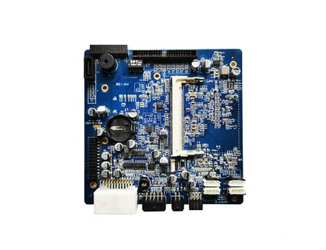
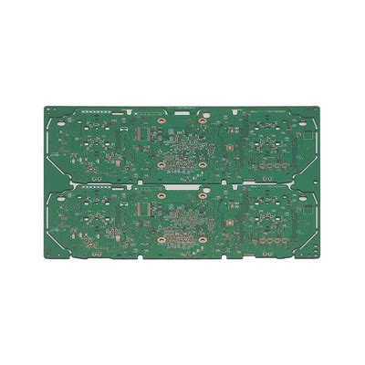
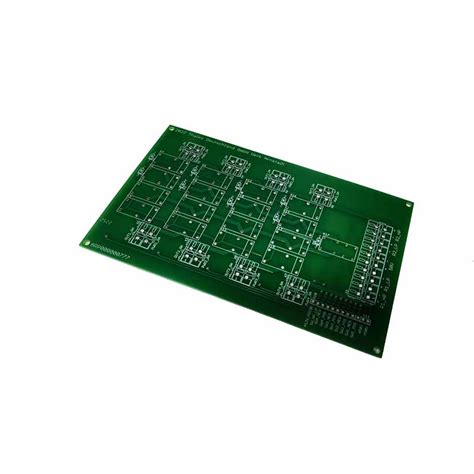
Double sided PCB assembly involves placing electronic components on both sides of a printed circuit board (PCB), which can lead to more compact and efficient designs. Understanding the fundamentals of this process is essential for achieving optimal performance in electronic projects. One of the key aspects to consider is the layout design; it is crucial to ensure that the arrangement of components maximizes space while minimizing interference and signal loss. This requires a thoughtful approach to both the front and back sides of the PCB. Moreover, mastering the soldering techniques is vital in double sided PCBA, as it impacts connectivity and reliability. Elements such as solder paste application, component placement, and thermal management play significant roles in ensuring a successful assembly. Additionally, familiarity with testing methods after assembly can help identify inconsistencies or faults early in development, allowing for corrective measures before final deployment. By comprehending these fundamental principles, one can streamline processes and enhance overall PCB assembly outcomes, ensuring both efficiency and reliability in complex electronic systems.
Designing Effective Layouts for Double Sided PCBs
When it comes to double sided PCB assembly, understanding how to design effective layouts is essential for achieving optimal functionality and reliability. A well-structured layout ensures that components are arranged efficiently, minimizing signal interference and promoting effective heat dissipation. One of the primary challenges faced in pcba is balancing space for components while maintaining proper trace routing.
To start, it’s critical to create a schematic diagram that outlines component placement. Consider the sizes and shapes of the components while ensuring there is enough space between them to avoid short circuits. Utilizing vias effectively allows for transitioning between the two sides of the board without cluttering the layout with excessive traces.
Here’s a simple table highlighting essential layout considerations:
| Layout Element | Considerations |
|---|---|
| Component Placement | Optimize spacing to prevent interference and allow for heat dissipation |
| Trace Routing | Aim for short, direct paths; prioritize vertical and horizontal routes |
| Vias | Use strategically to connect traces from top to bottom without overcrowding |
| Ground Planes | Incorporate ground planes where possible to reduce electromagnetic interference |
Moreover, incorporating design software equipped with simulation capabilities can help visualize potential issues before moving forward with production. Such tools not only assist in identifying problems but also allow for optimization of the overall layout, paving the way for a smoother assembly process.
Ultimately, meticulous attention to detail in your layout will enhance both performance and reliability in your double sided PCB assembly projects. As you gain experience, continually assess and refine your layouts based on feedback from practical testing to ensure that your final product meets high standards of quality and functionality.
The Soldering Process: Techniques and Best Practices
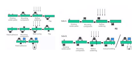
The soldering process in double sided PCB assembly (also known as PCBA) is crucial for ensuring the integrity and performance of electronic devices. When working with double sided PCBs, it is essential to select appropriate soldering techniques that can accommodate the complexity of components on both sides of the board. One effective method is the use of reflow soldering, which allows for precise temperature control, ensuring that solder paste is adequately melted to create reliable connections without damaging sensitive components.
Incorporating a vacuum pick-and-place system can enhance placement accuracy, reducing the likelihood of misalignment before the soldering process begins. Additionally, wave soldering can be a viable option for certain configurations where through-hole components are present. By selecting the proper solder mask and ensuring optimal temperatures during reflow or wave soldering, users can significantly improve joint reliability, minimizing defects.
Implementing best practices such as thorough pre-assembly inspections and utilizing enhanced cleaning methods prior to solder application will also contribute to better adhesion and fewer cold joints in the final product. Moreover, maintaining a clean work environment free from contamination is vital; any foreign particles could lead to increased failures during testing phases. By understanding these techniques and focusing on quality throughout the pcb assembly process, practitioners can achieve optimal performance and ensure high reliability across their electronic projects.
Testing Methods for Ensuring Reliability in PCBs
Ensuring the reliability of PCB assembly is critical for the long-term performance of any electronic device. Various testing methods play a significant role in assessing the functionality and durability of a board after assembly. One prominent technique is the use of Automated Optical Inspection (AOI), which allows for a visual examination of components on both sides of double sided PCBs without manual intervention. This method can quickly identify misalignments or soldering defects that may compromise performance. Additionally, functional testing is performed to ensure that the assembled PCBA operates as intended under real-world conditions, which includes verifying connections and voltage levels on various components. Moreover, leveraging environmental testing helps assess how the board withstands elements such as temperature fluctuations and humidity, which can be crucial for many applications. By incorporating these rigorous methods alongside comprehensive soldering techniques and layout design considerations, one can achieve robust reliability in double sided PCB assembly, ultimately enhancing the overall quality and performance of electronic projects.
Troubleshooting Common Issues in Double Sided PCB Assembly
When engaging in double sided PCB assembly, various challenges may surface that can hinder the overall efficiency and reliability of the pcba process. One common issue lies in alignment errors; misalignment of components can lead to poor solder joints or even circuit failure. To address this, utilizing precise placement techniques and reliable fixtures during assembly is vital. Additionally, solder bridging is a prevalent problem, particularly in densely populated boards where there are numerous narrow traces. Implementing controlled soldering techniques and optimizing the solder mask design can mitigate this risk substantially.
Another frequent concern involves the thermal management of a double sided assembly. Excessive heat can adversely affect component performance and longevity, particularly for sensitive parts located on the underside of the board. Employing effective thermal vias and ensuring that proper heat dissipation methods are integrated into the design will promote reliability and endurance.
Moreover, component integrity must be maintained throughout the assembly process. Damage during handling or from inappropriate soldering temperatures can lead to compromised performance. Hence, it is crucial to adopt best practices for handling sensitive components, coupled with thorough training for personnel involved in pcb assembly.
Lastly, systematic testing methods play an essential role in troubleshooting potential issues early on. Performing thorough inspections and leveraging automated optical inspection (AOI) systems can help identify defects before they escalate into larger problems. Overall, understanding these common challenges within double sided PCB assembly operations allows engineers to refine their techniques, thereby improving both performance and reliability for their electronic projects.
Materials Selection: Choosing the Right Components for Dual-sided Boards
When embarking on pcb assembly, one of the most critical stages is the selection of materials. Choosing the right components for dual-sided boards can significantly impact the overall performance and reliability of your pcba. It’s essential to consider factors such as component size, power requirements, and thermal characteristics. For instance, lower-profile components can save space on a double sided PCB, but they must also conform to strict thermal management guidelines to prevent overheating. Additionally, selecting components with compatible footprints ensures efficient layout, minimizing potential issues during soldering. Each component’s electrical properties should be meticulously evaluated; capacitors must be appropriately rated for voltage, while resistors need to match circuit requirements. By prioritizing quality and performance in material selection, you set a solid foundation for your double-sided PCB assembly, ultimately leading to more reliable and efficient electronic devices. It’s also beneficial to stay abreast of industry advancements in component technologies that can optimize both functionality and manufacturability in your designs.
Advanced Techniques for Enhancing Assembly Efficiency
Achieving high efficiency in pcb assembly requires a comprehensive understanding of various advanced techniques that streamline the entire process. First and foremost, integrating automated soldering methods, such as wave soldering and reflow soldering, can significantly enhance production speed while ensuring consistent quality in the solder joints. Furthermore, utilizing a dual-access layout minimizes the need for multiple handling steps during the assembly process, thus reducing assembly time. It is also beneficial to adopt specialized tools and equipment that are designed for PCBA tasks; these can improve accuracy and reduce human error. Another critical aspect is implementing rigorous quality control at each stage of the assembly process, using techniques such as X-ray inspection to evaluate hidden solder joints and ensure optimal functionality. Emphasizing proper training for technicians in these advanced methods also plays a vital role in enhancing overall assembly performance. By recognizing the value of efficient design principles alongside effective soldering techniques, engineers can significantly advance their pcb assembly practices while achieving greater reliability and performance in their electronic projects.
Case Studies: Successful Double Sided PCB Projects
Examining real-world applications of double sided PCB assembly (or PCBA) provides invaluable insights into effective strategies and methodologies employed by industry leaders. For instance, in the telecommunications sector, a major company successfully developed a dual-layer circuit board that optimized both performance and space. By meticulously designing the layout to include multiple components on both sides, they enhanced signal integrity while reducing the overall size of the device. The use of advanced soldering techniques played a crucial role in this success; reflow soldering was utilized to ensure consistent joints and minimize defects.
Similarly, in consumer electronics, a notable project involved creating a compact audio amplifier using double sided PCBs. The designers leveraged thermal management practices to effectively dissipate heat while allowing for dense component placement. Rigorous testing protocols were implemented post-assembly to ensure reliability and performance, which ultimately led to an innovative product that stood out in the marketplace. These case studies illustrate not only the versatility of PCB assembly but also emphasize the significance of strategic design considerations and robust processes in achieving optimal results in countless applications.
Conclusion
In summary, mastering double sided PCB assembly is essential for achieving optimal performance in your electronic projects. This process encompasses various key aspects, from designing effective layouts to selecting the appropriate materials that influence the overall success of your pcb assembly. The importance of understanding the soldering process cannot be overemphasized, as it significantly impacts the durability and functionality of the board. Moreover, employing rigorous testing methods ensures that every component operates as intended and meets reliability standards. By addressing common issues through a systematic troubleshooting approach, you can enhance the quality of your pcba projects. As technology evolves, embracing advanced techniques can further boost assembly efficiency and improve outcomes in your endeavors. Ultimately, investing time in these critical areas will lead to better-designed products that perform reliably and satisfy user expectations.
FAQs
What is double sided PCB assembly?
Double sided PCB assembly, or pcba, involves the process of mounting components on both sides of a printed circuit board. This assembly method allows for more complex circuit designs and greater functionality.
What are the advantages of using double sided PCBs?
Double sided pcbs provide several advantages, including increased component density and reduced space requirements. This is crucial for designs where space is at a premium, facilitating more compact and efficient electronic devices.
How can I ensure efficient layout design in double sided PCB assembly?
Efficient layout design in double sided pcb assembly can be achieved by careful planning, including the placement of components to minimize signal interference and optimize routing. Utilizing appropriate software tools can significantly aid in this process.
What soldering techniques are best for double sided PCBs?
For double sided PCBA, techniques like reflow soldering and manual soldering can be employed effectively. It’s important to choose the right technique based on the components used and to ensure proper heat application to avoid damage.
How do I test my assembled double sided PCB for reliability?
Testing methods such as functional testing, in-circuit testing, and thermal imaging are effective for ensuring reliability in your double sided assemblies. Regular testing should be implemented throughout the production process.
What common issues should I troubleshoot in double sided PCB assembly?
Common issues in double sided PCB assembly include solder bridging, insufficient solder joints, and misaligned components. Identifying these problems early can prevent costly errors down the line.


