Mastering HDI PCB Fabrication Techniques for Efficient Design

Key Takeaways
In the realm of HDI PCB fabrication, understanding the vital components and processes can significantly impact your project’s success. By focusing on microvias and their applications, you can increase efficiency in your designs. Microvias allow for greater routing flexibility, which is essential when dealing with compact and complex circuit layouts. Furthermore, emphasizing the importance of stack-up planning in HDI design not only enhances reliability but also plays a crucial role in determining the PCB manufacturing cost. Utilizing advanced techniques can lead to improved reliability in your designs.
When choosing PCB manufacturing companies, consider those that apply innovative strategies to reduce costs without sacrificing quality. Developing a cost-effective PCB manufacturing business model is crucial to staying competitive while maintaining high standards. By investing in modern fabrication techniques, you can accelerate time-to-market, ensuring your products meet market demands swiftly.
“Efficient design not only minimizes costs but also maximizes product reliability.”
In summary, prioritizing these key areas will lead to successful HDI PCB implementations that align with market needs and enhance overall effectiveness in PCB manufacturing.
Introduction to HDI PCB Fabrication
High-Density Interconnect (HDI) printed circuit boards (PCBs) represent a significant advancement in pcb manufacturing, allowing designers to create more compact, reliable, and efficient electronic devices. As you delve into HDI PCB fabrication, it’s essential to understand the intricacies involved in this process. The use of microvias, which are tiny holes that connect different layers of the board, is one crucial technique that enhances pcb manufacturability. By utilizing microvias, you can maximize space on your PCB while improving electrical performance and signal integrity. Additionally, effective stack-up planning is vital in ensuring that your pcb manufacturing business can support all required functionalities while maintaining durability. This approach not only promotes reliability but also reduces the overall manufacturing cost. As competition grows among various pcb manufacturing companies, mastering these techniques becomes increasingly important for delivering superior products that meet market demands swiftly. By implementing advanced HDI techniques and focusing on efficient design strategies, you can accelerate your time-to-market and position your business for ongoing success in the evolving landscape of electronic design and manufacturing.
Understanding Microvias: Benefits and Applications
When it comes to HDI PCB fabrication, one of the most pivotal features to consider is the use of microvias. These tiny drill holes, often measuring less than 150 microns in diameter, provide significant advantages in efficient design and space management. The introduction of microvias allows for higher layer counts without increasing the PCB size, thus making them essential for compact and sophisticated electronics. This becomes particularly crucial as you aim to tap into the benefits of advanced pcb manufacturing techniques that can lead to elevated functionality in smaller packages.
One of the main benefits of using microvias is their contribution to improved signal integrity. By reducing the length of traces and minimizing their exposure to noise, microvias enhance the overall performance of your circuit boards. This is particularly beneficial for high-frequency applications where performance can degrade due to longer trace lengths or electromagnetic interference. Moreover, employing microvias can effectively lower pcb manufacturing costs as they facilitate denser layouts that require fewer materials while also streamlining assembly processes.
In terms of applications, you may find that pcb manufacturing companies are increasingly adopting microvia technology in products ranging from smartphones to medical devices. Their capabilities support not only miniaturization but also facilitate improved thermal management by allowing heat dissipation paths directly through multiple layers. With their ability to support complex designs while keeping manufacturing costs manageable, microvias are undeniably a game-changer in the realm of HDI PCBs.
In summary, incorporating microvias into your designs not only enhances reliability but also opens up vast opportunities in advancing your pcb manufacturing business forward. Leveraging such advanced techniques will ultimately allow you to meet growing consumer demands while ensuring that your PCBs maintain high performance, lower costs, and shorter time-to-market timelines.
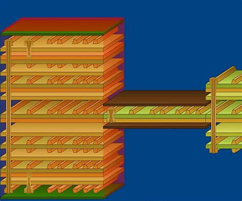
Importance of Stack-Up Planning in HDI Design
In the realm of HDI PCB fabrication, stack-up planning stands as a critical component that can significantly influence the overall performance and reliability of your design. Effective stack-up design involves thoughtful consideration of the arrangement of layers within the PCB manufacturing process, which directly impacts signal integrity, thermal performance, and manufacturability. By strategically planning your stack-up, you can optimize space utilization through the use of microvias, enhancing not just physical layout but also electrical performance.
When engaging with PCB manufacturing companies, it’s vital to articulate your stack-up requirements clearly. A well-planned stack-up allows for the implementation of high-density interconnections, which not only facilitates advanced functionality but also leads to potential cost reduction due to efficient material usage and streamlined fabrication processes. Additionally, investing time in stack-up planning minimizes rework and revisions during production stages—elements that can escalate the PCB manufacturing cost significantly.
Understanding how to effectively arrange your layers empowers you to address crucial factors such as impedance control and electromagnetic interference. This meticulous attention to detail helps ensure that your product remains reliable under varying operational conditions while accelerating your time-to-market for new innovations in a competitive PCB manufacturing business landscape. By prioritizing stack-up planning in your HDI designs, you set a strong foundation for successful product outcomes that meet both technical specifications and market demands.
Advanced Techniques for Enhancing Reliability
To ensure enhanced reliability in HDI PCB fabrication, several groundbreaking techniques have emerged. Microvias, a critical feature of HDI PCBs, are not only essential for accommodating densely packed circuitry but also contribute significantly to improving structural integrity. When you incorporate microvias in your design, it can lead to optimized performance by reducing signal loss and enhancing thermal dissipation, which are crucial in high-frequency applications. Moreover, stack-up planning plays a pivotal role in reliability; it involves strategic arrangement of the PCB layers to minimize electromagnetic interference and ensure optimal impedance control. By understanding the nuances of stack-up planning, you can tailor the design to meet specific performance criteria while conforming to industry standards.
Further, implementing advanced materials known for their thermal management properties can significantly impact long-term reliability. Selecting components that withstand higher temperatures will also ensure your PCBs endure various operational stresses without degradation. Each of these aspects contributes holistically to a reduced PCB manufacturing cost and consolidates reliability across the lifecycle of your product, ultimately benefiting your PCB manufacturing business. Additionally, when partnered with reputable PCB manufacturing companies, these techniques not only reinforce quality but also make collaboration more fruitful, expediting development processes while maintaining adherence to rigorous standards necessary for successful market entry. Thus, by focusing on these advanced techniques, you enhance not only the reliability of your products but also position your business favorably within the competitive landscape of PCB manufacturing.
Cost Reduction Strategies in HDI PCB Fabrication
When exploring cost reduction strategies in HDI PCB fabrication, it is crucial to adopt a comprehensive approach that addresses several key factors. First and foremost, consider optimizing your choice of material. Selecting components that offer the best price-to-performance ratio is essential. Additionally, working closely with reputable PCB manufacturing companies can lead to bulk purchasing opportunities and more favorable rates for larger orders. Also, leveraging modern design software can facilitate better layouts, ultimately reducing manufacturing time and associated costs.
You may want to focus on minimizing the number of layers in your HDI designs, which directly affects the PCB manufacturing cost. A reduction in layers can lead to less material usage and improved efficiency in production timelines. Another crucial element is the implementation of effective stack-up planning, which streamlines both design and production processes, ensuring that the right balance of thickness and dielectric material is achieved while maintaining signal integrity.
Incorporating automated processes into your PCB manufacturing business can drastically decrease labor costs and human error, thus enhancing overall production efficiency. Moreover, regularly reviewing your supply chain for potential cost savings—whether through better supplier negotiations or alternative sourcing—can make a significant impact. By focusing on these strategies and maintaining an adaptive mindset, you can effectively reduce expenses while enhancing the quality of your HDI printed circuit boards.
Accelerating Time-to-Market Through Efficient Design
In the fast-paced world of electronics, accelerating time-to-market can significantly enhance your competitive edge. Efficient design practices are at the heart of this acceleration, particularly in HDI PCB fabrication. By leveraging advanced techniques such as microvias and optimized stack-up planning, you can streamline your designs and reduce development time. These innovations not only lead to improved reliability but also mitigate the pcb manufacturing cost, allowing you to achieve efficiency without compromising quality. As you navigate the realm of pcb manufacturing companies, consider adopting strategies that focus on minimizing unnecessary iterations and embracing rapid prototyping. This approach not only speeds up the overall process but also aligns with the capabilities of modern pcb manufacturing business models, which prioritize quick turnaround times. Ultimately, enhancing your design efficiency will allow you to respond swiftly to market demands and foster a more dynamic product development cycle.
Case Studies: Successful HDI PCB Implementations
Analyzing real-world cases of HDI PCB fabrication provides valuable insights into the practical applications and benefits of advanced design techniques. One prominent example involves a major telecommunications company that sought to enhance the performance of its devices while controlling pcb manufacturing costs. By leveraging microvias and optimized stack-up planning, this company managed to create more compact and reliable circuit boards, ultimately improving signal integrity. The result was a 20% reduction in both weight and size, which led to significant improvements in product performance.
Another illustrative case is that of an automotive electronics manufacturer that aimed to reduce the overall time-to-market for its new line of electric vehicles. By embracing cutting-edge pcb manufacturing technologies, such as laser drilling for microvias, they were able to achieve faster prototyping and refinement cycles. This approach not only streamlined their development process but also allowed them to respond more swiftly to market demands, enhancing their competitive edge.
Moreover, this manufacturer partnered with specialized pcb manufacturing companies that focused on innovative fabrication techniques. Through collaboration, they discovered cost-effective materials specifically designed for high-density interconnects (HDI), which contributed positively to their bottom line while ensuring the durability necessary for automotive applications.
These case studies highlight how integrating advanced HDI PCB fabrication techniques can lead to significant operational benefits. They showcase a clear path for other businesses looking to enhance their product offerings without compromising on quality or increasing their pcb manufacturing costs significantly. Emphasizing continuous improvement in design and manufacturing processes illustrates how companies can maintain a competitive outlook in an ever-evolving market landscape while executing efficient designs that resonate with both performance standards and economic viability.
Future Trends in HDI PCB Manufacturing
As you look toward the horizon of HDI PCB manufacturing, several important trends are emerging that could reshape your approach to design and production. First, the rise of advanced automation technologies is streamlining processes within PCB manufacturing companies, leading to enhanced efficiency and precision. This automation reduces human error and can significantly lower PCB manufacturing costs, allowing you to allocate resources toward innovation rather than just production overhead. Additionally, as the demand for compact devices increases, there’s a growing emphasis on microvias and multilayer designs which can improve space utilization while maintaining performance. Furthermore, sustainability practices are becoming critical in the PCB manufacturing business, with eco-friendly materials and processes gaining traction. This shift not only aligns with global initiatives but can also attract a more environmentally conscious consumer base. Keeping an eye on these trends empowers you to adapt your strategies proactively, ensuring that your designs remain competitive in an evolving market landscape. Thus, embracing these advancements will be key to enhancing reliability and facilitating faster time-to-market for your innovative products.
Conclusion
In summary, mastering HDI PCB fabrication techniques is essential for engineers and designers aiming to stay competitive in the fast-evolving electronics market. By understanding the nuances of microvias and effective stack-up planning, you can significantly improve the reliability and functionality of your designs. Furthermore, adopting advanced methods aimed at enhancing performance not only streamlines your processes but also lowers the overall pcb manufacturing cost. As you navigate through choices among various pcb manufacturing companies, stay informed about trends that favor efficiency and cost-effectiveness in your pcb manufacturing business to ensure timely delivery of high-quality products. Ultimately, whether you’re a seasoned professional or a newcomer, these techniques are crucial for accelerating your time-to-market while meeting customer demands. Embracing this knowledge positions you to lead in developing next-generation electronic solutions that harness the full potential of advanced PCB technologies.
FAQs
What is HDI PCB fabrication?
HDI PCB fabrication stands for High-Density Interconnector Printed Circuit Board fabrication. It involves advanced manufacturing techniques that allow for more components to be packed densely onto a board, resulting in smaller, lighter, and more efficient circuit designs.
What are microvias and why are they important?
Microvias are small vias that connect layers in a PCB. They are crucial for pcb manufacturing as they enable greater routing density and support complex designs while reducing the overall size of the board.
How does stack-up planning affect HDI design?
Stack-up planning plays a pivotal role in pcb manufacturing cost management. It determines how layers are arranged, impacting both the electrical performance and physical characteristics of the PCB. A well-planned stack-up can lead to reduced signal integrity issues and enhance reliability.
What strategies can I implement to reduce costs in HDI PCB fabrication?
To cut down pcb manufacturing costs, consider optimizing your design for fewer layers, using standard sizes, or choosing reliable yet cost-effective materials. Collaborating with specialized pcb manufacturing companies can also help identify savings opportunities without compromising quality.
How can I accelerate my project’s time-to-market using HDI techniques?
By utilizing advanced design tools that streamline the layout process and choosing pcb manufacturing business partners known for their efficiency, you can significantly shorten your production timeline. Effective communication with suppliers early in the design phase also helps avoid delays.