Mastering PCB Assembly: A Comprehensive Guide to Creation and Design
Key Takeaways
When embarking on the journey of PCB assembly (often abbreviated as PCBA), it is crucial to grasp several key concepts that underpin successful creation and design. Understanding the basic terminologies and processes involved can significantly impact the quality and efficiency of your projects. A well-structured PCB assembly process begins with meticulous planning, focusing on the design’s compatibility with manufacturing capabilities. Emphasizing the significance of key components, one must prioritize careful selection, layout optimization, and circuit integrity to ensure a reliable end product. In addition, employing effective techniques for pcb assembly, such as surface mount technology (SMT) or through-hole mounting, can enhance both production speed and accuracy. Furthermore, addressing common challenges that arise during PCBA, like alignment issues or component variations, is vital in maintaining high standards in your work. By leveraging best practices for testing and quality assurance, you significantly bolster the reliability of your boards. Ultimately, staying informed about future trends in PCB design will help you adapt to advancements in technology and maintain a competitive edge in this rapidly evolving field.
Introduction to PCB Assembly: Understanding the Basics
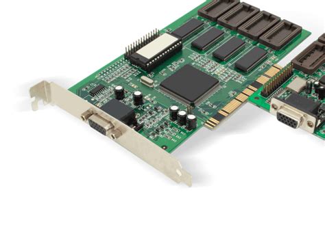
PCB assembly, or PCBA, is a fundamental process in the realm of modern electronics that involves the careful integration of electronic components onto a printed circuit board. This process begins with the design of the PCB, where engineers lay out the circuitry and determine the placement of components. The creation of a functional PCB is critical, as it serves as the backbone for any electronic device. Understanding this assembly process helps in ensuring that projects are not only efficient but also reliable.
When engaging in pcb assembly, it’s essential to familiarize oneself with various techniques and methodologies that enhance this creation process. Such techniques might include surface mount technology (SMT) and through-hole technology (THT), each having its own set of advantages depending on the application. Moreover, attention to detail during design phase plays a significant role in minimizing common challenges faced during assembly, such as misalignment or poor solder joints.
Ultimately, mastering PCBA requires a comprehensive understanding of both theory and practical skills, allowing engineers to troubleshoot problems effectively and consistently achieve high-quality results in their electronic projects. As technology continues to advance, staying attuned to best practices in PCB creation helps ensure that products are not only competitive but also poised for success in an ever-evolving market landscape.
The Role of PCB Design in Modern Electronics
In the realm of modern electronics, PCB design plays a pivotal role in the overall functionality and reliability of devices. By intricately mapping out circuit pathways, PCB assembly becomes a seamless process that aligns with foundational engineering principles and user requirements. A well-structured design not only enhances pcba efficiency but also minimizes signal interference, which can lead to costly malfunctions.
Furthermore, effective PCB design incorporates considerations for thermal management and component placement, which are critical to ensuring the longevity of electronic gadgets. “A thoughtfully designed PCB can significantly reduce assembly time and errors, ultimately benefiting both manufacturers and end-users.” > Therefore, investing time in meticulous design stages can yield not just immediate advantages but long-term success in product development.
Additionally, with advancements in technology, designers now have access to sophisticated software tools that facilitate the creation of more complex pcba layouts while maintaining ease of assembly. This evolution underscores the transformative impact of focused PCB design, which equips engineers to respond adeptly to the demands of an ever-evolving technological landscape. As such, appreciating the intricate connection between design choices and overall performance is essential for anyone engaged in the electronic manufacturing sector.
Key Components of a Successful PCB Creation Process
The process of PCB assembly requires careful consideration of several key components to ensure the final product is both efficient and reliable. One of the primary elements is design integrity, which influences how well the components fit together and function within the circuit. Selecting high-quality materials plays a vital role as well; the choice between different types of substrates, for instance, affects thermal conductivity and performance under varying environmental conditions. Additionally, a thorough understanding of electrical characteristics is essential for optimal component placement and routing, thereby reducing interference and signal degradation.
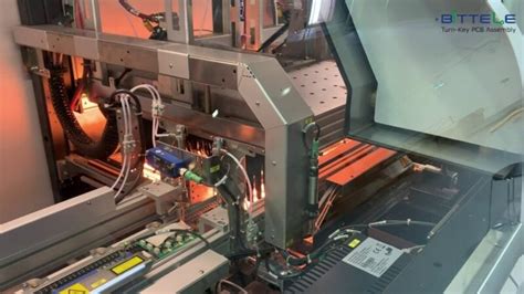
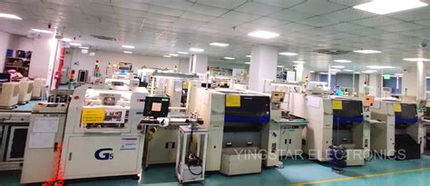
Another significant aspect is manufacturing capabilities; selecting a contractor that specializes in PCBA not only guarantees that they have experience with various materials but also with advanced manufacturing processes such as surface mount technology (SMT) or through-hole technology. This expertise can greatly enhance production efficiency while minimizing defects. Furthermore, integrating robust testing methods throughout the creation process—such as automatic optical inspection (AOI) or in-circuit testing (ICT)—ensures that any potential issues are identified early on, promoting a reliable end product. By focusing on these core elements, designers can effectively navigate the complexities of PCB assembly, leading to successful outcomes in their electronic projects.
Techniques for Efficient PCB Assembly
Efficient PCB assembly (also known as PCBA) relies on a combination of precise techniques and a well-structured workflow. One fundamental approach is the use of automated assembly processes, which can significantly reduce the time and labor involved in producing PCBs. Automation not only enhances production speed but also minimizes human error, contributing to higher quality outcomes.
Additionally, implementing a just-in-time inventory system ensures that components are available precisely when needed, thus reducing waste and optimizing costs. To visualize this process, consider the following table which outlines essential steps in efficient PCB assembly:
| Step | Description | Benefits |
|---|---|---|
| 1 | Component Sourcing | Ensures all necessary parts are on hand |
| 2 | Automated Placement | Reduces placement time and error rates |
| 3 | Soldering Techniques | Enhances reliability and strength of joints |
| 4 | Quality Control Checks | Identifies defects early in the process |
Moreover, maintaining optimal workspace organization can lead to an efficient workflow. By ensuring that tools and materials are easily accessible, teams can minimize downtime during the assembly process. Effective communication among team members is also crucial; when everyone understands their roles and responsibilities clearly, it fosters a smoother operation overall.
In conclusion, mastering these techniques in PCB assembly leads to more streamlined production processes while guaranteeing high standards of quality. Organizations that invest time into refining their assembly strategies will ultimately achieve greater reliability in their electronic projects.
Common Challenges in PCB Assembly and How to Overcome Them
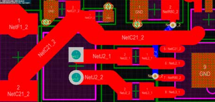
In the realm of pcb assembly, professionals often encounter several challenges that can impede the creation and functionality of electronic devices. One of the most prevalent issues is component misalignment during the assembly process. This can lead to poor connections and, ultimately, device failure. To counter this, utilizing automated pick-and-place machines with precision calibration can significantly enhance accuracy and reduce human error.
Another challenge involves thermal management. Excessive heat can damage components, particularly in densely packed pcba designs. Implementing effective heat dissipation techniques such as heat sinks or thermal vias in your layout can mitigate this risk, ensuring longevity and reliability in your assemblies.
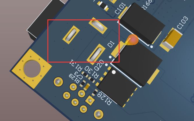
Moreover, soldering defects such as cold joints or solder bridges are common pitfalls that must be addressed. Employing rigorous inspection methods like X-ray imaging or Automated Optical Inspection (AOI) can help detect these flaws early in the process, allowing for timely corrections.
Lastly, maintaining a comprehensive documentation process is critical for identifying problems when they arise. Proper records of each stage in the pcb assembly lifecycle facilitate troubleshooting and improvements, ultimately leading to higher quality outcomes. By being proactive and implementing these strategies, you can navigate the common hurdles of PCB assembly effectively while creating robust and dependable electronic products.
Best Practices for Testing and Quality Assurance in PCBs
Effective pcb assembly relies heavily on stringent testing and quality assurance practices to ensure the final product meets industry standards. A well-structured approach to pcba quality testing begins with establishing a set of comprehensive guidelines that account for different stages of the assembly process. Initially, implementing rigorous visual inspections can help catch potential defects early on, such as misplaced components or improper soldering techniques. Utilizing automated optical inspection (AOI) further enhances detection capabilities, scrutinizing the board for any anomalies that may affect performance.
In addition to visual checks, functional testing is critical. This step involves evaluating the assembled PCB under operational conditions to ensure it behaves as intended. Test jigs or specialized equipment can be employed for this purpose, specifically designed to simulate real-world scenarios where the pcb assembly will be utilized.
Moreover, thermal and reliability testing plays a pivotal role in validating the long-term performance of pcba products. Subjecting PCBs to thermal cycling or vibration tests can help identify weaknesses that could lead to failures over time.
Lastly, documentation throughout the testing phases should be meticulously maintained. This practice not only aids in traceability but also facilitates continuous improvement by providing valuable insights for future projects. Adhering to these best practices ensures that your pcb assembly delivers products that are not only reliable but also positioned for success in competitive markets.
Future Trends in PCB Design and Assembly
As the electronics industry continues to evolve, the future of PCB assembly (or PCBA) is being shaped by several significant trends that promise to enhance both efficiency and performance. One of the primary drivers is the increasing demand for miniaturization. As devices become smaller, manufacturers are focusing on advanced techniques that allow for densely packed components without compromising design integrity. Innovations such as surface mount technology (SMT) are becoming more prevalent, as they facilitate the placement of components in a more compact manner, catering to the growing need for handheld devices.
Moreover, the integration of smart technology into PCBs is gaining traction. This trend involves embedding sensors and connectivity features directly into the PCB design process, thus enabling devices to communicate and gather data autonomously. Companies are exploring how to leverage the Internet of Things (IoT) within their PCBA processes, enhancing interactivity and functionality.
Another noteworthy trend is the adoption of automated solutions in PCB assembly. Automation not only increases production speed but also improves precision and consistency across large batches. The use of robotics and AI-driven tools in inspection processes has begun to revolutionize quality assurance in products, ensuring higher standards are met before reaching consumers.
Sustainability is also an integral focus area moving forward; manufacturers are seeking eco-friendly materials and processes that minimize waste and energy consumption. The shift toward green manufacturing practices is not only a response to consumer demand but also a proactive measure towards regulatory compliance.
In summary, these trends illustrate that the landscape of PCB assembly is rapidly changing as technology advances. Embracing these developments will be crucial for businesses aiming to stay competitive in an increasingly complex environment where efficiency, sustainability, and innovation dictate success in the field of PCBA.
Conclusion: Ensuring Reliability and Success in Your Projects
In the dynamic field of PCB assembly (PCBA), ensuring the reliability and success of your projects requires a careful blend of design proficiency and assembly expertise. By adhering to established best practices throughout the creation process, from initial design to final assembly, you can enhance both the performance and durability of your printed circuit boards. This involves selecting high-quality materials, employing precise manufacturing techniques, and implementing rigorous testing protocols. Understanding how each component interacts within the overall system is crucial; this holistic perspective allows for effective troubleshooting when issues arise. Additionally, utilizing innovative tools and software for simulation can considerably mitigate risks early in the design phase. Ultimately, maintaining a focus on efficiency and reliability not only contributes to cost-effective production but also paves the way for future advancements in technology. By embracing these principles within your PCBA processes, you position your projects for long-term success in an ever-evolving landscape of modern electronics.
Conclusion: Ensuring Reliability and Success in Your Projects
In the intricate realm of pcb assembly, ensuring reliability and success is paramount. Throughout this guide, we have delved into various facets of PCB assembly, emphasizing the importance of robust design principles and meticulous creation processes. Effective pcba requires not just technical knowledge but also a deep understanding of the interaction between components and their roles in the overall functionality of the circuit. By adhering to best practices outlined in our previous sections, such as efficient assembly techniques and diligent quality assurance methods, you can minimize common challenges that may arise during production. As technologies evolve, staying abreast of future trends in PCB design will be critical. This proactive approach not only enhances the performance and durability of your projects but also ensures they stand up successfully in today’s competitive electronics market. With careful planning and execution in your pcb assembly efforts, you can foster innovations that resonate well into the future.
FAQs
What is PCB assembly?
PCB assembly, often referred to as PCBA, is the process of soldering components onto a printed circuit board (PCB) to create a complete electronic device. This crucial step ensures that all parts work together seamlessly, enabling the functionality of modern electronics.
What materials are commonly used in PCB assembly?
The materials used in PCB assembly typically include copper for the circuit traces, various types of substrates like FR-4 for the board itself, and solder for joining components. With advancements in technology, materials like flexible substrates and conductive inks are also gaining popularity.
What are the key steps in the PCB assembly process?
The key steps in the PCB assembly process include design layout creation, component placement, soldering, and testing. Each step plays an essential role in ensuring that the final product meets industry quality standards and performs as intended.
How can I ensure quality in my PCB assembly?
To ensure quality in your PCBA, it’s essential to implement best practices such as rigorous testing at each stage of production, using high-quality materials and components, and adhering to reliable design specifications. Regular audits of your manufacturing process can also help maintain consistency.
What common issues occur during PCB assembly?
Common issues during PCB assembly may include solder bridging, component misalignment, and thermal stress. Understanding these potential challenges allows designers and manufacturers to develop strategies to minimize their occurrence.
For more resources on PCB Assembly, please click here: Andwin PCB Assembly