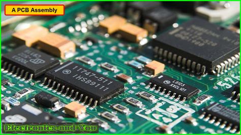
Mastering PCB Manufacturing: Expert Tips for Efficient Prototyping

Key Takeaways
When navigating PCB manufacturing, understanding core efficiency drivers helps you avoid common pitfalls. Start by evaluating rapid prototyping capabilities—modern PCB manufacturing companies employ laser direct imaging and automated optical inspection to slash lead times by 40-60%. For cost management, analyze material waste patterns and batch ordering strategies; industry benchmarks show these can reduce PCB manufacturing cost by up to 22% without compromising quality.
| Factor | Traditional Approach | Optimized Approach |
|---|---|---|
| Prototyping Time | 10-15 days | 3-5 days (with automation) |
| Cost Efficiency | High material waste | Panelization + JIT ordering |
| Quality Assurance | Manual inspections | AOI + X-ray layer scanning |
Your PCB manufacturing business benefits from integrating real-time testing protocols like in-circuit and functional testing, which cut defect rates by 30%. For scaling, consider hybrid partnership models—combining local prototyping hubs with offshore mass production units balances speed and PCB manufacturing cost effectively. Prioritize suppliers with ISO 9001-certified workflows to ensure consistency across global operations.
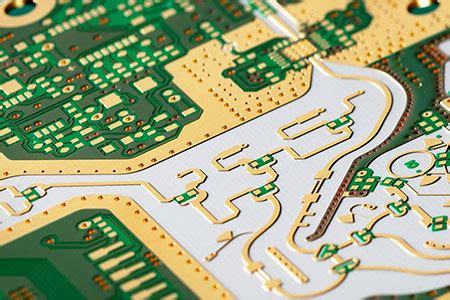
Rapid PCB Prototyping Techniques Explained
When accelerating PCB manufacturing timelines, your approach to prototyping can make or break project schedules. Leading PCB manufacturing companies prioritize design validation through iterative testing, leveraging advanced CAD tools to identify layout flaws early. By adopting modular design principles, you reduce rework cycles—a critical factor in controlling PCB manufacturing cost.
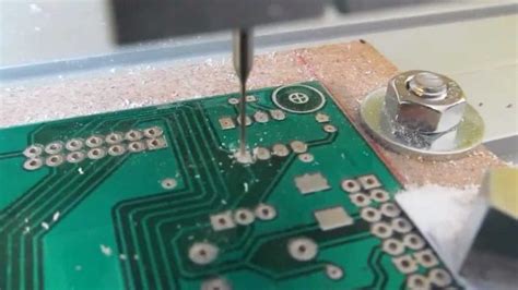
Modern techniques like laser direct imaging (LDI) enable tighter tolerances for high-density interconnects, while additive processes such as inkjet printing allow rapid layer stacking. For time-sensitive projects, partnering with PCB manufacturing business units offering 24-hour turnaround ensures functional prototypes within days. However, speed shouldn’t compromise reliability: automated optical inspection (AOI) systems verify trace integrity before moving to full production.
To balance urgency and quality, integrate design-for-manufacturability (DFM) checks into your workflow. This minimizes post-prototype adjustments, preserving both timelines and budgets. As you refine designs, consider material compatibility—a misstep here could inflate PCB manufacturing cost during scaling. Transitioning seamlessly from prototyping to mass production requires aligning with partners who standardize fabrication parameters across batches, a strategy we’ll explore further in cost optimization.
Cost Optimization Strategies for PCB Production
When working with PCB manufacturing companies, balancing quality and PCB manufacturing cost requires a strategic approach. Start by optimizing your design files—simplifying layer counts, minimizing board sizes, and avoiding unnecessary via structures can reduce material waste and processing time. Many PCB manufacturing providers offer design-for-manufacturability (DFM) reviews to identify cost-saving opportunities early.
Another critical lever is batch ordering. Consolidating multiple prototypes or small batches into larger production runs often unlocks volume discounts without compromising turnaround times. For recurring projects, establish long-term partnerships with PCB manufacturing business partners to negotiate favorable pricing tiers.
Material selection also plays a pivotal role. While high-frequency laminates or specialized substrates may be essential for niche applications, standard FR-4 materials typically offer the best cost-performance ratio for most projects. Always verify material specifications with your manufacturer to avoid over-engineering.
Finally, leverage automated quoting tools provided by modern PCB manufacturing services. These platforms instantly compare pricing across different quantities and specifications, helping you make data-driven decisions. Pair this with rigorous testing protocols to catch defects early—rework expenses often dwarf initial savings from cutting corners.
By aligning design choices, production scales, and supplier partnerships, you create a streamlined cost structure that supports both prototyping agility and scalable PCB manufacturing cost management.
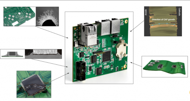
Ensuring Quality Assurance in PCB Manufacturing
Achieving consistent quality in PCB manufacturing requires a systematic approach that integrates design verification, material validation, and rigorous testing. Leading PCB manufacturing companies begin by cross-checking design files against industry standards like IPC-6012 to eliminate errors before production. Automated optical inspection (AOI) systems then scan each layer during fabrication, flagging microscopic defects that could compromise functionality.
To balance PCB manufacturing cost with reliability, prioritize suppliers offering certified materials with traceable lot numbers. For high-frequency or thermal-sensitive applications, impedance testing and thermal cycling become critical to validate performance under real-world conditions. Partnering with a PCB manufacturing business that employs X-ray inspection for hidden flaws in multilayer boards adds another layer of assurance.
Post-assembly, in-circuit testing (ICT) and functional testing simulate operational environments to catch latent failures. Implementing statistical process control (SPC) tools helps monitor variability across batches, ensuring long-term consistency. By embedding these protocols early, you reduce rework expenses and strengthen your product’s market reputation—proving that quality isn’t an added cost but a strategic safeguard in scalable PCB manufacturing.
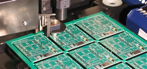
Streamlining PCB Assembly Workflow Processes
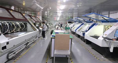
To optimize your PCB manufacturing workflow, start by mapping every stage of assembly—from component procurement to final testing. Process bottlenecks often emerge in manual tasks like solder paste application or part placement, which can be mitigated through automated systems. Leading PCB manufacturing companies integrate pick-and-place machines and automated optical inspection (AOI) to reduce human error and accelerate throughput.
"Implementing just-in-time inventory management minimizes storage costs and ensures fresher components, directly impacting PCB manufacturing cost efficiency."
When collaborating with partners, standardize communication protocols to avoid misinterpretations. Use digital twin simulations to pre-validate designs, cutting rework cycles by up to 30%. For PCB manufacturing business scalability, adopt modular production lines that adapt to varying batch sizes without downtime.
Prioritize design-for-manufacturability (DFM) checks early to eliminate compatibility issues. Pairing this with real-time data analytics allows you to monitor yield rates and adjust workflows dynamically.
Finally, consolidate quality checkpoints post-reflow and post-assembly. Combining inline testing with final functional verification ensures defects are caught early, reducing scrap rates. By aligning these strategies, you create a leaner, more responsive workflow that balances speed and precision.
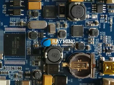
Advanced Materials Selection for Optimal PCBs
Choosing the right materials is a cornerstone of successful PCB manufacturing, directly influencing performance, reliability, and long-term durability. When working with PCB manufacturing companies, you’ll encounter a range of substrate options—from standard FR-4 to high-frequency laminates like Rogers or PTFE. Each material offers distinct trade-offs in thermal conductivity, dielectric properties, and mechanical stability, which must align with your application’s demands. For instance, high-speed designs require low-loss materials to minimize signal degradation, while industrial applications prioritize heat-resistant substrates to withstand harsh environments.
Balancing PCB manufacturing cost with quality starts by evaluating material specifications against operational requirements. Opting for cheaper FR-4 might reduce upfront expenses, but specialized laminates could lower failure rates in critical systems, ultimately benefiting your PCB manufacturing business through reduced rework. Collaborating closely with suppliers ensures access to cutting-edge materials like halogen-free alternatives or flexible polyimide films, which cater to evolving trends in miniaturization and sustainability.
Remember, material selection isn’t just about technical specs—it’s about foreseeing how choices impact assembly compatibility, testing protocols, and lifecycle management. By prioritizing advanced materials early in the design phase, you lay the groundwork for PCBs that excel in both performance and manufacturability.
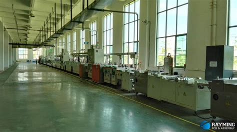
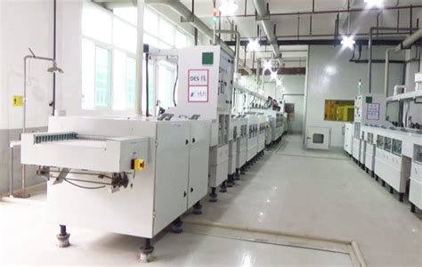
Leveraging Automation in PCB Fabrication
When optimizing your PCB manufacturing workflow, automation isn’t just a luxury—it’s a strategic necessity. Modern PCB manufacturing companies now integrate automated optical inspection (AOI) systems and robotic assembly lines to minimize human error while accelerating production cycles. By deploying AI-driven design validation tools, you can identify potential flaws in Gerber files before prototyping, reducing material waste and PCB manufacturing cost by up to 30%.
For instance, automated panelization software streamlines board layouts to maximize substrate utilization, directly impacting your PCB manufacturing business profitability. Advanced pick-and-place machines with machine vision ensure micron-level precision for surface-mount components, even in high-mix production runs. This shift toward closed-loop feedback systems allows real-time adjustments during etching or soldering, maintaining consistent quality across batches.
However, adopting automation requires balancing upfront investments with long-term gains. Partnering with vendors offering modular solutions lets you scale capabilities incrementally—critical for smaller enterprises. Remember: the goal isn’t just faster output, but creating a resilient framework that adapts to evolving design complexities while keeping per-unit costs competitive.
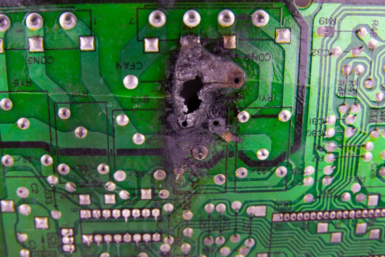
Testing Protocols for Reliable PCB Performance
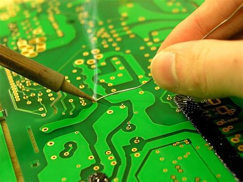
To ensure your PCB manufacturing process delivers consistent results, implementing rigorous testing protocols is non-negotiable. Leading PCB manufacturing companies prioritize a multi-layered approach, combining automated and manual inspections to catch defects early. Start with in-circuit testing (ICT) to verify electrical connectivity, followed by automated optical inspection (AOI) to identify soldering flaws or misaligned components. For high-density designs, X-ray inspection becomes critical to examine hidden connections like BGA joints.
Balancing PCB manufacturing cost with quality requires strategic test sequencing. For instance, running AOI before functional testing reduces rework expenses by 30–40% in typical PCB manufacturing business operations. Environmental stress tests, including thermal cycling and vibration simulations, further validate board durability under real-world conditions. When selecting a partner, prioritize firms offering traceability reports—these documents not only ensure compliance with industry standards but also streamline troubleshooting if field failures occur.
By integrating these protocols, you create a feedback loop that refines both design and production phases, aligning with the broader goals of cost efficiency and scalability outlined earlier in your project lifecycle.
Global Partnership Models for Efficient Scaling
When expanding your PCB manufacturing operations, strategic alliances with specialized PCB manufacturing companies can accelerate growth while managing PCB manufacturing cost pressures. By aligning with partners in key geographic regions, you gain access to localized expertise, advanced production facilities, and streamlined supply chains—critical factors for scaling your PCB manufacturing business without compromising quality. Joint ventures and licensing agreements, for instance, allow you to leverage existing infrastructure while sharing R&D investments, reducing capital expenditure risks.
For example, partnering with a fabrication facility in Southeast Asia could cut material procurement costs by 15–20% while maintaining compliance with international standards. Similarly, technology transfer partnerships enable access to proprietary manufacturing techniques, enhancing your competitive edge. To ensure alignment, establish clear performance metrics for quality control and cost efficiency, and prioritize partners with proven expertise in your target markets. This approach not only optimizes production scalability but also creates redundancy in your supply chain, mitigating regional disruptions. By integrating global partnerships into your growth strategy, you transform geographical and operational challenges into opportunities for sustainable expansion.
Conclusion
As you refine your approach to PCB manufacturing, the culmination of strategic planning and technical execution becomes evident. Partnering with reputable PCB manufacturing companies ensures access to cutting-edge technologies while maintaining control over PCB manufacturing cost. Whether you’re scaling a PCB manufacturing business or optimizing prototypes, prioritizing quality assurance and process automation remains non-negotiable.
The journey from design to production hinges on balancing speed, precision, and affordability. By adopting data-driven testing protocols and leveraging global partnership models, you mitigate risks and enhance scalability. Remember that successful PCB manufacturing isn’t just about meeting specifications—it’s about anticipating challenges in material selection, assembly workflows, and regulatory compliance.
As the industry evolves, staying informed about emerging materials and fabrication techniques will keep your projects competitive. Invest in relationships with suppliers who align with your cost and quality objectives, and never underestimate the value of iterative testing. In doing so, you transform complex manufacturing hurdles into opportunities for innovation and growth.
Frequently Asked Questions
How do experienced engineers select the right PCB manufacturing companies for prototyping?
Look for suppliers with ISO-certified facilities, proven turnaround times, and transparent PCB manufacturing cost structures. Prioritize partners offering design-for-manufacturing (DFM) analysis to prevent costly revisions.
What drives PCB manufacturing cost variations between projects?
Material choices (high-frequency substrates vs standard FR-4), layer count, surface finishes, and order volume significantly impact pricing. Bulk orders typically reduce per-unit costs by 15-30% in PCB manufacturing business operations.
Can automation truly improve PCB manufacturing consistency?
Yes. Automated optical inspection (AOI) and robotic soldering systems achieve <0.1% defect rates in advanced facilities. This reduces rework expenses by up to 40% while maintaining strict quality benchmarks.
How do global PCB manufacturing companies handle supply chain risks?
Leading providers maintain multi-region production hubs and buffer inventories of critical components. Some offer dual-sourcing strategies for materials like copper-clad laminates to ensure uninterrupted workflows.
What certifications matter most when evaluating PCB manufacturing partners?
IPC-A-600 (workmanship standards) and UL listing are essential. For specialized applications, request IATF 16949 (automotive) or ISO 13485 (medical) compliance to meet industry-specific safety requirements.
Ready to Optimize Your PCB Production?
Explore how our PCB manufacturing solutions accelerate prototyping while cutting costs. Click here to request your customized quote or discuss technical specifications with our engineering team.