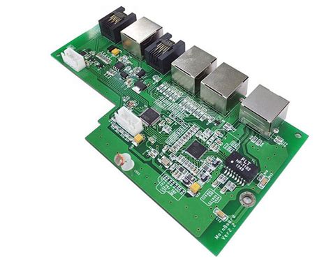
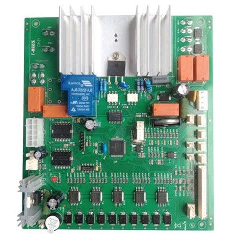
Mastering Precision in PCB Board Assembly

Key Takeaways
Achieving precision in PCB assembly requires a systematic approach that integrates advanced techniques with rigorous quality assurance. At the core of PCBA excellence lies precision component placement, where micron-level accuracy ensures optimal electrical performance and reliability. Equally critical are soldering accuracy methods, such as reflow and wave soldering, which minimize defects like cold joints or bridging.
To maintain consistency, modern PCB assembly workflows incorporate automated inspection systems, including AOI (Automated Optical Inspection) and X-ray testing, which detect flaws invisible to the human eye. These systems are particularly vital in aerospace-grade and medical electronics applications, where failure rates must approach zero.
| Industry | Critical Standards | Inspection Focus |
|---|---|---|
| Aerospace | IPC-A-610 Class 3 | Thermal cycling resilience |
| Medical Electronics | ISO 13485 | Signal integrity under sterilization |
| Consumer Electronics | IPC-A-610 Class 2 | High-volume throughput efficiency |
Transitioning between industries demands adaptable PCBA strategies. For instance, while consumer electronics prioritizes cost-effective scaling, medical devices require biocompatible materials and traceability. By aligning process controls with application-specific demands, manufacturers ensure that every PCB assembly meets both functional and regulatory benchmarks without compromising efficiency.
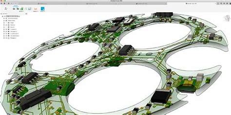
Precision PCB Component Placement
Achieving micrometer-level accuracy in PCB assembly begins with meticulous component placement, where even minor deviations can compromise functionality in high-stakes applications like aerospace or medical devices. Modern pick-and-place machines leverage vision systems and programmable nozzles to position surface-mount devices (SMDs) with tolerances under 0.05mm. For mixed-technology boards, combining automated placement with manual adjustments ensures alignment for both fine-pitch ICs and through-hole components.
Tip: Always verify component orientation against the Gerber file during placement to avoid polarity-related failures post-soldering.
Critical factors influencing placement precision include PCBA substrate flatness, solder paste viscosity, and environmental controls to minimize thermal expansion shifts. Advanced systems integrate real-time feedback loops, adjusting placement parameters based on laser profilometry data. This is particularly vital for RF shielding cans or BGA packages, where even 10µm misalignment can degrade signal integrity.
Transitioning seamlessly to soldering, precise placement sets the foundation for reliable solder joints, reducing rework rates. Automated optical inspection (AOI) systems later validate positional accuracy, creating a closed-loop quality chain essential for mission-critical electronics.
Accurate Soldering Techniques for PCBs
Achieving precision in PCB assembly hinges on mastering soldering techniques that ensure electrical reliability and mechanical stability. Modern PCBA processes employ two primary methods: reflow soldering for surface-mount devices (SMDs) and wave soldering for through-hole components. Reflow soldering relies on precisely controlled temperature profiles to melt solder paste, creating uniform connections without thermal damage to sensitive components. For through-hole parts, wave soldering immerses board bottoms in a molten solder wave, requiring exact conveyor speed and flux application to prevent bridging or cold joints.
Critical to both methods is solder paste stencil design, which dictates deposit volume and alignment. Advanced PCB assembly lines use laser-cut stencils with ±10μm accuracy to optimize paste distribution. Additionally, nitrogen-environments during reflow reduce oxidation, enhancing joint integrity—a practice vital for aerospace or medical PCBA where failure risks are unacceptable.
Automated optical inspection (AOI) systems now complement manual checks, scanning solder joints for defects like insufficient wetting or tombstoning. For high-density boards, X-ray inspection verifies hidden connections under ball grid arrays (BGAs). These protocols, paired with IPC-A-610 standards, ensure PCB assembly meets industry-specific tolerances, whether for consumer electronics miniaturization or ruggedized aerospace circuitry. By integrating precise process controls with cutting-edge inspection, manufacturers eliminate variability while scaling production—a balance critical to modern electronics manufacturing.
Quality Control in PCB Assembly Processes
Effective PCB assembly relies on rigorous quality control protocols to ensure reliability across high-stakes industries like aerospace and medical devices. At the core of these protocols is traceability, which tracks components from procurement to final testing, minimizing risks of counterfeit parts or process deviations. Automated optical inspection (AOI) systems scan PCBA units for soldering defects, misaligned components, or insufficient solder joints, while X-ray inspection identifies hidden flaws in ball grid arrays (BGAs) or multilayer boards.
Statistical process control (SPC) tools analyze production data in real time, flagging anomalies in parameters such as reflow oven temperatures or paste deposition volumes. For mission-critical applications, environmental stress screening (ESS) subjects assemblies to thermal cycling, vibration, and humidity tests, simulating decades of operational wear in hours. Compliance with IPC-A-610 and J-STD-001 standards ensures solder joint integrity, with cross-sectional analysis validating internal connections.
By integrating these measures, manufacturers achieve first-pass yield rates exceeding 99.5%, reducing rework costs and accelerating time-to-market. This systematic approach not only aligns with aerospace-grade and medical electronics requirements but also scales efficiently for high-volume consumer PCB assembly, maintaining consistency across diverse production environments.
Automated Inspection Systems for PCB Perfection
Modern PCB assembly processes demand rigorous quality assurance, driving the adoption of intelligent automated inspection systems to eliminate human error and ensure consistency. Advanced PCBA production lines integrate automated optical inspection (AOI) and X-ray inspection (AXI) technologies to scrutinize solder joint integrity, component alignment, and trace continuity at micron-level resolutions. These systems leverage machine learning algorithms to compare real-time scans against golden board references, flagging deviations like tombstoning, bridging, or insufficient solder volume. For high-reliability sectors such as aerospace electronics and medical devices, in-circuit testing (ICT) and flying probe testers validate functional performance under simulated operational stresses, ensuring compliance with IPC-A-610 and J-STD-001 standards. The shift toward Industry 4.0 further enables closed-loop feedback, where inspection data automatically recalibrates pick-and-place machines or reflow ovens, creating self-optimizing PCBA workflows. By combining 3D SPI (solder paste inspection) with AOI, manufacturers achieve near-zero defect rates while maintaining throughput speeds exceeding 20,000 components per hour—a critical balance for consumer electronics mass production. This multi-layered inspection paradigm not only safeguards against field failures but also builds traceability archives for regulatory audits and root cause analysis, cementing automated systems as the cornerstone of precision-driven PCB assembly.
Aerospace-Grade PCB Assembly Standards
In aerospace applications, PCB assembly demands adherence to rigorous standards that surpass conventional requirements. The industry relies on specifications such as IPC-A-610 (Class 3) and AS9100, which govern everything from material selection to final inspection. High-reliability components must withstand extreme temperatures, vibrations, and radiation, necessitating precision in PCBA processes like solder joint integrity and conformal coating application.
Aerospace-grade assemblies prioritize traceability, with detailed documentation for every component, including lot numbers, certifications, and thermal profiles. Automated optical inspection (AOI) and X-ray systems are critical for detecting micro-cracks or voids in solder joints, which could compromise performance in mission-critical systems. Additionally, cleanroom environments and electrostatic discharge (ESD) controls minimize contamination risks during PCB assembly.
To meet these standards, manufacturers often employ advanced techniques such as high-density interconnect (HDI) layouts and microvia drilling, ensuring compact yet robust designs. Collaboration with aerospace engineers during the design-for-manufacturability (DFM) phase further optimizes reliability. By integrating these protocols, PCBA providers deliver boards capable of enduring the harsh conditions of aviation, satellite, and defense systems without failure.
Medical Electronics PCB Quality Protocols
In PCB assembly for medical devices, adherence to stringent quality protocols is non-negotiable. Unlike consumer electronics, medical applications demand zero-tolerance for defects due to their critical role in patient care. PCBA processes here must align with regulatory standards such as ISO 13485 and IEC 60601, which govern design validation, material biocompatibility, and sterilization compatibility. For instance, traceability is enforced through serialized component tracking, ensuring every resistor, capacitor, and integrated circuit can be traced back to its manufacturing batch.
Automated optical inspection (AOI) and X-ray testing are prioritized to detect micro-soldering flaws or misalignments invisible to the naked eye. Additionally, accelerated life testing simulates years of operational stress within weeks, verifying long-term reliability under extreme conditions like humidity or temperature fluctuations. Manufacturers also implement cleanroom PCB assembly environments to prevent particulate contamination, which could compromise sensitive implantable devices. By integrating these protocols, PCBA suppliers guarantee that medical electronics meet not only functional specifications but also the ethical imperative of patient safety.
Consumer Electronics PCB Optimization Strategies
In contrast to aerospace or medical applications, consumer electronics demand PCB assembly strategies that balance cost-efficiency with high-volume performance. Optimizing PCBA for devices like smartphones or wearables requires meticulous attention to component density and thermal management, as compact designs often push the limits of material and manufacturing tolerances. A critical focus lies in design-for-manufacturability (DFM) principles, where layout engineers collaborate with PCB assembly teams to minimize signal interference and ensure reliable solder joints in ultra-thin profiles.
Advanced reflow soldering profiles and selective use of lead-free alloys help maintain durability under frequent thermal cycling, a common stressor in consumer devices. Additionally, automated optical inspection (AOI) systems are calibrated to detect micro-scale defects in PCBA, such as tombstoning or insufficient solder paste deposition, which could compromise long-term functionality. To address power consumption challenges, designers often integrate low-loss substrates and optimize trace routing to reduce parasitic capacitance—key for extending battery life in portable electronics.
Finally, rigorous environmental stress testing simulates real-world conditions, from humidity exposure to mechanical shock, ensuring PCB assembly integrity aligns with consumer expectations for reliability. By harmonizing these strategies, manufacturers achieve the delicate equilibrium between affordability and precision demanded by today’s fast-paced consumer markets.
Advanced Soldering Methods in PCB Manufacturing
Modern PCB assembly relies on advanced soldering techniques to ensure electrical reliability and mechanical stability, particularly in high-performance applications. Reflow soldering remains a cornerstone of PCBA processes, utilizing precisely controlled temperature profiles to melt solder paste while minimizing thermal stress on sensitive components. For surface-mount devices (SMDs), stencil printing accuracy ensures uniform solder deposition, critical for micro-BGA and QFN packages. In mixed-technology boards, wave soldering complements reflow methods, addressing through-hole components with optimized solder wave height and contact time to prevent bridging.
Emerging methods like laser soldering offer localized heat application, ideal for temperature-sensitive medical or aerospace electronics. Nitrogen-enriched reflow ovens further enhance joint quality by reducing oxidation, a practice increasingly adopted in automotive PCB assembly. Automated optical inspection (AOI) systems now integrate with soldering equipment to detect defects such as cold joints or tombstoning in real time, aligning with IPC-A-610 standards. For ultra-fine-pitch components, selective soldering systems provide targeted precision, minimizing collateral heat exposure.
The shift toward lead-free alloys (e.g., SAC305) demands tighter process controls, as melting points and wetting characteristics differ from traditional tin-lead solders. Advanced PCBA workflows now incorporate predictive analytics to optimize furnace settings, reducing defects by up to 30% in high-density interconnect (HDI) designs. These innovations underscore the balance between process scalability and defect mitigation, ensuring robust performance across industries demanding millimeter-level precision.
Conclusion
The pursuit of precision in PCB assembly hinges on harmonizing advanced techniques with rigorous quality frameworks. As industries like aerospace, medical, and consumer electronics demand increasingly reliable PCBA outcomes, manufacturers must prioritize traceability and process repeatability. By integrating automated optical inspection (AOI) systems and adhering to industry-specific protocols, defects can be minimized at critical stages—from component placement to final soldering validation.
Success in PCB assembly also relies on balancing human expertise with technological innovation. While robotic soldering ensures micron-level accuracy, skilled technicians remain essential for troubleshooting complex layouts or fine-tuning thermal profiles. Furthermore, adopting statistical process control (SPC) methods strengthens quality assurance, enabling real-time adjustments that align with medical-grade or aerospace-certified standards.
Ultimately, achieving flawless PCBA requires a commitment to continuous improvement. By leveraging data-driven insights from automated testing and fostering collaboration between design and production teams, manufacturers can meet the evolving demands of high-reliability applications while maintaining cost efficiency. This holistic approach not only elevates product performance but also solidifies trust in mission-critical electronic systems.
FAQs
What defines precision in PCB assembly?
Precision in PCBA involves micron-level accuracy in component placement, adherence to thermal profiles during soldering, and strict compliance with design specifications. This ensures reliable electrical connections and minimizes defects in high-stakes industries like aerospace and medical devices.
How do automated inspection systems enhance PCB quality control?
Automated optical inspection (AOI) and X-ray systems detect microscopic flaws—such as solder bridges or misaligned components—that manual checks might miss. These systems integrate with PCB assembly lines to provide real-time feedback, reducing rework and ensuring compliance with IPC-A-610 standards.
Why are soldering techniques critical for consumer electronics?
Consumer devices demand compact, high-density PCBA designs. Techniques like reflow soldering and selective soldering maintain signal integrity while preventing thermal damage to sensitive components, ensuring longevity in products like smartphones and wearables.
What certifications matter for aerospace-grade PCB assembly?
Aerospace PCBA requires adherence to AS9100D and NASA-STD-8739.4, emphasizing traceability, rigorous testing, and resistance to extreme temperatures. These protocols ensure reliability in mission-critical applications like avionics and satellite systems.
Ready to Optimize Your PCB Assembly Process?
For tailored solutions in PCB assembly that meet aerospace, medical, or consumer electronics standards, please click here to explore our advanced PCBA capabilities and technical support.