Mastering the Art of Electronics: A Comprehensive Guide to PCB Manufacturing
Key Takeaways
In exploring PCB manufacturing, it’s essential to grasp several key insights that can influence your projects and decisions. First and foremost, understanding the PCB manufacturing process helps you better communicate your ideas to PCB manufacturing companies. This includes not only the technical aspects but also the logistical factors that can affect the PCB manufacturing cost. When engaging with a PCB manufacturing business, consider factors such as turnaround time, material quality, and production capabilities. Having this knowledge empowers you to make informed choices that align with your specific project needs. Additionally, being aware of best practices in design and production will improve the overall quality of your PCBs, ensuring that they meet both functional and aesthetic standards. By mastering these takeaways related to PCB manufacturing, you enhance not only your designs but also foster more productive collaborations with industry professionals.
Introduction to PCB Manufacturing: The Foundation of Modern Electronics
The world of PCB manufacturing serves as a cornerstone for all modern electronic devices, from simple household gadgets to advanced technological systems. Understanding the intricacies of how printed circuit boards are created is crucial for anyone involved in electronics. During the pcb manufacturing process, the journey begins with the transformation of innovative ideas into tangible PCB layouts. This initial phase requires a blend of creativity and technical skills, as circuit designers must meticulously consider factors such as functionality and manufacturability.
As you venture further into pcb manufacturing, you’ll discover that choosing reputable pcb manufacturing companies can significantly impact the quality and reliability of your final product. A detailed comparison of their services might reveal varying pcb manufacturing costs, which can help you budget effectively for your pcb manufacturing business. When selecting a partner, pay attention not only to pricing but also to their production capabilities, lead times, and customer support.
Ultimately, investing time in understanding each stage of the PCB production process equips you with valuable insight that enhances your ability to make informed decisions. Familiarity with terms such as etching, solder mask application, and layer alignment will not only prepare you for effective communication with manufacturers but also enhance your confidence in navigating this complex landscape. As you progress through the nuances of PCB design and production, remember that thorough preparation today lays the groundwork for successful electronics tomorrow.
“The best designs emerge from understanding both creativity and technology—ensure to balance both in your PCB ventures.”
The Design Process: Transforming Ideas into PCB Layouts
The journey of pcb manufacturing begins with a well-defined design process, where your innovative ideas are translated into precise PCB layouts. This initial phase is crucial as it sets the foundation for the entire pcb manufacturing process. You need to use specialized software tools to create a schematic representation of your circuit design. These tools allow you to define various elements, including components, connections, and electrical requirements, ensuring that your design meets both functional and aesthetic considerations.
As you create your layout, it is essential to pay attention to the pcb manufacturing companies‘ guidelines regarding trace widths and spacing in order to avoid common pitfalls that could lead to increased pcb manufacturing costs. You should also consider the capabilities of chosen manufacturers; some companies may have specific restrictions based on their equipment. It’s wise to familiarize yourself with design rules that pertain to different materials and technologies used in the pcb manufacturing business.
Furthermore, think about how your layout impacts the overall performance of the circuit; factors such as signal integrity and thermal management can significantly affect functionality. As you refine your design, iterative testing can help you identify areas for improvement. In doing so, you’re not just laying down tracks for electrical currents; you are crafting a reliable framework that plays a critical role in the eventual performance of your electronic device.
In conclusion, mastering the art of PCB design equips you with the tools necessary for successful pcb manufacturing while enhancing collaboration with manufacturers throughout your project journey. As you engage in this creative process, consider exploring more about potential partners and services offered by leading manufacturers at Andwin PCB who can help bring your ideas to life efficiently.
From File to Film: Preparing for PCB Production
As you embark on the journey of PCB manufacturing, the transition from digital design files to physical production begins with crucial preparatory steps. Understanding this phase is pivotal to ensuring that your layout translates accurately into a functional board. First, you need to ensure that your design files adhere to specific PCB manufacturing guidelines, often referred to as Design for Manufacture (DFM) rules. These guidelines help mitigate errors that could arise during production and are crucial when dealing with PCB manufacturing companies.
Once validated, your digital designs are converted into a film format, which serves as a photo mask for printed circuit board proliferation. This process involves generating layers that will ultimately define the conductive paths and features of your board. Each layer is carefully aligned and checked to ensure precision—essential factors that influence the overall PCB manufacturing cost. The quality of this film is significant; any defect can lead to discrepancies in the final product.
Moreover, integrating advanced software tools aids in managing complexities associated with your PCB manufacturing business. Tools focused on automating file checks can catch potential errors early in the process, thus avoiding costly revisions down the line. As you progress with these preparations, remember that meticulous attention at this stage not only streamlines production but also enhances the reliability and efficacy of your final product, setting a robust foundation for subsequent steps in the PCB manufacturing process.
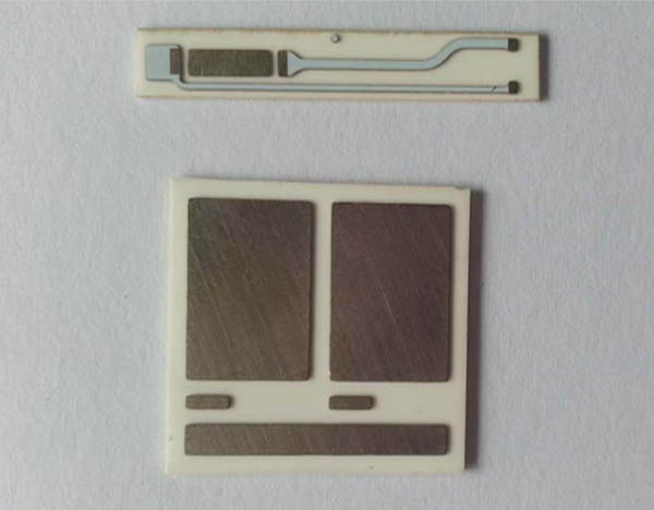
Inner Layer Printing and Copper Path Creation
In the realm of pcb manufacturing, the process of inner layer printing and copper path creation is pivotal in ensuring that your printed circuit boards function reliably. This stage involves transferring the electrical designs onto substrate materials, wherein precise layering is crucial. Initially, photoresist material is applied to the inner layers of the PCB. When exposed to UV light, this material hardens in specific areas, forming a protective layer that defines where copper will remain after etching. This critical step helps in achieving high-quality copper paths that are essential for electrical connectivity.
The consistency of this process can significantly affect both the performance and durability of your circuit board. Using high-accuracy imaging techniques allows for detailed designs to be accurately represented on the copper layer, minimizing errors that could escalate pcb manufacturing costs. Being aware of these nuances can help you when engaging with pcb manufacturing companies, ensuring you select a partner capable of delivering quality results.
Furthermore, in any pcb manufacturing business, understanding how sophisticated technologies affect inner layer creation can impact both design and function. As you navigate through this intricate phase, keep in mind how well-executed copper paths not only ensure efficiency but also contribute to the overall longevity of your PCB. By familiarizing yourself with these processes, you position yourself to better evaluate potential suppliers and their capabilities within today’s competitive landscape.
Drilling and Plating: Connecting Circuitry
In the realm of pcb manufacturing, the processes of drilling and plating are pivotal for establishing reliable electrical connections on your circuit boards. Once you have completed the inner layer printing and copper path creation, it is time to drill holes through the layers of the PCB. These holes will accommodate plated-through holes (PTH), which are necessary for connecting various layers of the circuit. As you explore pcb manufacturing companies, it’s essential to understand that precision is crucial in this stage; any inaccuracies in drilling can lead to electrical failures or short circuits.
After drilling, the next step is plating, where a thin layer of copper is deposited into these holes. This process creates a conductive pathway that links the layers of your PCB, effectively integrating all components into a unified circuit board. The quality and efficiency of these processes can significantly influence your overall pcb manufacturing cost, so selecting a proficient pcb manufacturing business can make all the difference in ensuring your project meets both budgetary and performance requirements. By mastering these techniques, you’ll be well-equipped to excel in your PCB endeavors, ready to navigate any complexities that come with modern electronics design.
Final Etching and Solder Mask Application
In the pcb manufacturing process, the final etching phase is where the magic truly happens. After the inner layers have been printed and drilled, it’s time to remove any unnecessary copper from the board. This step ensures that only the desired copper pathways remain, effectively detailing your circuit’s layout. Utilizing a mixture of solutions, you facilitate a clean and precise etching process that results in highly defined patterns essential for electrical performance. Following this, you apply a solder mask, which serves as a protective layer over your board. This coating not only prevents unwanted solder from bridging conductors during assembly but also enhances the durability of your PCB by protecting it against environmental factors.
Choosing proper solder mask application techniques is critical in optimizing your PCB for various applications — from consumer electronics to complex industrial tools. Many pcb manufacturing companies offer advanced options such as electrostatic or screen printing methods for solder mask application. Understanding these variants can aid you in managing your pcb manufacturing costs, as some techniques may be more budget-friendly than others while still ensuring quality.
Incorporating these essential elements into your pcb manufacturing business model can greatly influence both performance and longevity of your products. Your knowledge of etching and soldering processes prepares you to make informed decisions about design optimizations, thereby enhancing fit-for-purpose outcomes and maximizing production efficiency. Through attention to detail in these final stages of production, you create boards that not only meet but exceed industry standards, setting a solid foundation for successful electronic devices.
Quality Assurance: Testing and Inspection Methods
In the realm of PCB manufacturing, ensuring high-quality standards is crucial for the reliability and performance of electronic products. You will encounter various testing and inspection methods that play an integral role in maintaining quality throughout the PCB manufacturing process. Initially, visual inspections allow you to detect major defects, such as misalignments or physical damages. Once the physical checks are completed, you can utilize advanced techniques like Automated Optical Inspection (AOI) to systematically verify component placement and solder joint quality.
Furthermore, conducting electrical tests is essential to confirm that each PCB functions correctly. You might opt for in-circuit testing (ICT) or functional testing (FT), depending on your specific requirements. The latter ensures that the PCB operates as intended in its real-world application. Understanding the PCB manufacturing cost also involves factoring in these essential quality assurance measures, as thorough testing can prevent costly failures down the line.
Choosing reliable PCB manufacturing companies is another vital aspect; ensure they have robust quality assurance protocols in place to guard against defects and ensure safety compliance. As you delve deeper into your PCB manufacturing business, remember that a commitment to rigorous testing and inspection not only elevates your product’s reliability but also strengthens customer trust in your brand. By adhering to these practices, you position yourself for long-term success in an increasingly competitive landscape.
Best Practices for Selecting a PCB Manufacturer
When it comes to pcb manufacturing, selecting the right manufacturer can significantly impact the quality and efficiency of your project. You should start by evaluating the pcb manufacturing companies based on their experience and reputation in the industry. A well-established company often indicates reliability and adherence to industry standards. Additionally, consider their capabilities—do they offer a variety of services that align with your specific needs? For instance, if you require complex designs, confirm that they have the technology and expertise necessary for intricate pcb manufacturing processes.
Next, you’ll want to assess the pcb manufacturing cost. While it may be tempting to choose the lowest bid, remember that quality matters tremendously in electronics production. A manufacturer that provides competitive pricing without compromising on quality is ideal. Look for detailed quotes that clarify what is included in the price; hidden fees can inflate your budget unexpectedly. Furthermore, don’t overlook customer support. A responsive team can be invaluable in addressing any concerns you might have during the pcb manufacturing business process.
Lastly, check for certifications and compliance with international standards—this ensures their processes are up to par with regulatory requirements, which is crucial for maintaining product integrity. By taking these factors into account, you can make a well-informed decision and ultimately enhance the success of your electronics projects through superior pcb manufacturing solutions.
Conclusion
In summary, understanding PCB manufacturing is crucial for anyone involved in the world of electronics. You have learned how the journey of a printed circuit board begins with a strong design foundation and evolves through various stages, including inner layer printing, drilling, and final etching. Each step contributes to the overall quality of the final product, making it essential to familiarize yourself with the intricate details of this process. By exploring various PCB manufacturing companies, you can compare their offerings and determine which align best with your specific needs and budget. Additionally, it’s worth contemplating the PCB manufacturing cost, which can vary significantly depending on factors such as complexity, materials used, and production volume. Understanding these aspects will empower you to make informed decisions in your PCB manufacturing business, ensuring that you achieve optimal results for your electronic projects. Equipped with this knowledge, you can approach PCB design and production with greater confidence, ready to tackle each challenge that comes your way in this fascinating industry.
FAQs
In your journey through PCB manufacturing, you may find yourself with a variety of questions. Understanding the nuances can be crucial for the success of your projects, whether you are a hobbyist or part of a larger pcb manufacturing business. One common inquiry pertains to the pcb manufacturing cost—how is it determined? Typically, costs are influenced by factors such as design complexity, material selection, layer count, and production volume. Thus, choosing the right pcb manufacturing companies aligned with your budgetary constraints is essential.
Another frequently asked question relates to turnaround times. Each pcb manufacturing company has its timelines based on their workflow and capabilities. It’s wise to check these aspects early to avoid potential delays in your projects. Moreover, the quality assurance process is often a point of concern; ensure that the company you select implements stringent testing and inspection protocols to meet your performance expectations.
As you navigate these questions, remember that understanding best practices in pcb manufacturing can greatly enhance your efficiency and output quality. Continuous research and communication with manufacturers will help you make informed decisions tailored to your specific needs.
Enhance Your Knowledge on PCB Manufacturing
For further exploration into PCB manufacturing and to refine your understanding of various nuances in this domain, please click here. You’ll find resources that can significantly aid in navigating the intricacies involved in designing and producing printed circuit boards effectively.