Mastering the Art of PCB Assembly Drawings: A Comprehensive Guide
Key Takeaways
Mastering the art of PCB assembly drawings requires attention to several critical elements that ensure your designs are both precise and efficient. Essential tools are the backbone of any successful PCBA project, from computer-aided design (CAD) software to comprehensive libraries of electronic components. Embracing best practices, such as maintaining clear and consistent labeling, can prevent errors and streamline the manufacturing process. Avoiding common pitfalls, such as insufficient documentation or unclear instructions, is vital for ensuring your designs are seamlessly translated from concept to production. Understanding these fundamentals will set both novices and experienced professionals on a path to elevate their pcb assembly skills significantly.
Introduction to PCB Assembly Drawings
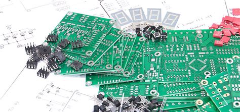
Creating PCB assembly drawings is an essential step in the design and manufacturing process of printed circuit boards (PCBA). These drawings provide a detailed map that conveys critical information about the placement of components, routing of traces, and other necessary specifications to ensure a successful assembly. A well-crafted PCB assembly drawing not only aids in reducing errors but also streamlines communication between designers, engineers, and production teams. By using specialized tools and adhering to industry standards, you can create precise and efficient drawings that seamlessly translate from concept to production. This guide will explore the importance of accurate PCBA drawings and the various elements that contribute to superior assembly outcomes, whether you are a novice stepping into the field or an experienced professional looking to refine your skills.
Essential Tools for Creating PCB Assembly Drawings
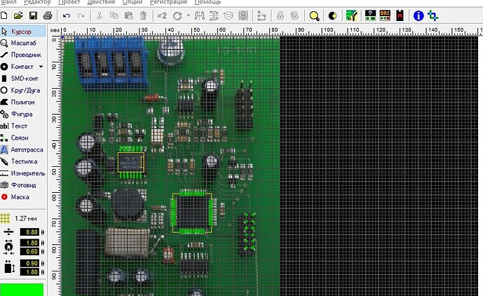
When creating PCB assembly drawings, having the right tools is crucial. These tools not only streamline the design process but also ensure precision and clarity in your diagrams. To begin with, CAD software is indispensable. Programs like Altium Designer, Eagle, and KiCAD offer various features tailored for detailed PCBA work. They provide libraries of components, which can be easily incorporated into your designs.
Another vital tool is a high-resolution scanner or camera, used for capturing clear images of component layouts and placements. These visuals can be integrated into your assembly drawings, offering a realistic guide that enhances understanding.
Furthermore, employing design verification tools will assist in error-checking your PCB designs. These include DRC (Design Rule Check) software, which helps identify layout inconsistencies or rule violations before they translate into costly production errors.
Here’s a quick overview of essential tools:
| Tool | Description |
|---|---|
| CAD Software | Used for designing and drafting PCB layouts |
| High-Resolution Scanner/Camera | Captures clear images for reference |
| Design Verification Tools | Ensures designs meet predefined standards |
By incorporating these essential tools into your workflow, you can achieve superior accuracy and efficiency in your PCB assembly drawings, whether you’re working on simple or complex designs.
Best Practices for Accurate and Efficient PCB Assembly Drawings
Creating accurate and efficient PCB assembly drawings is essential in ensuring seamless product development and manufacturing. Start by ensuring that all components are uniquely identified with component labels. This aids in proper part placement and reduces confusion during assembly. Use clear and concise notations to indicate the orientation and polarity of components, as these factors are critical for the correct functioning of the device.
Tip: “Always cross-reference your schematic with the assembly drawing to catch any discrepancies early in the process.”
Incorporating detailed silk screen layers is equally important; they provide additional visual guidance and can be especially helpful when dealing with densely populated boards. Remember to include fiducial markers, which are essential for automated assembly processes like pick-and-place machines.
Another best practice is to include a comprehensive Bill of Materials (BOM) alongside your PCB assembly drawing. This document should list all part numbers, quantities, and descriptions, ensuring that every item needed for the PCBA is accounted for.
Use software tools that allow for layer visualization so you can verify all elements are correctly positioned before finalizing the drawing. Consistent use of symbols and terminology throughout your documentation will enhance readability and reduce potential errors.
Suggestion: “Engage in regular design reviews with manufacturing teams to ensure your PCB assembly drawing aligns with production capabilities.”
By following these best practices, you can create clear, detailed, and effective PCB assembly drawings that streamline production workflows and ensure high-quality outcomes.
Detailed Steps to Create a Precise Assembly Drawing
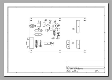
Creating a precise assembly drawing for a printed circuit board (PCB) involves several methodical steps, crucial for ensuring that your design is accurately interpreted and executed in production. Begin by selecting the right software tools that cater to your pcb assembly needs, such as CAD programs specifically designed for PCB layouts. Next, import your finalized PCB design and start by annotating each component with its part number, orientation, and placement details. This step includes the use of reference designators that are clearly visible and non-overlapping to prevent confusion during manufacturing.
Ensure that every element of the drawing provides clarity; this means detailing all the layers of the PCB, including the top and bottom views if applicable. Highlight the solder mask and paste layers distinctly and indicate any specific pcba requirements such as thermal reliefs or specialized tolerances. It’s vital to include a Bill of Materials (BOM) alongside your drawing which lists all components used in the assembly with exact specifications.
Additionally, incorporate any mechanical drawings that exhibit hole placements, cut-outs, or mounting points crucial for enclosures or final product assembly. Use color-coding effectively to distinguish between different types of components and signals if your design software permits it.
Lastly, finalize your assembly drawing by conducting a thorough review process. This should involve cross-verifying each part of your design against the original schematic diagrams to ensure consistency and checking for any potential zones where errors could arise during manufacturing. By adhering strictly to these steps, you can achieve a highly detailed and precise PCB assembly drawing that facilitates seamless translation from concept to production.
Common Pitfalls to Avoid in PCB Assembly Drawings
Creating accurate and efficient PCB assembly drawings is essential for the smooth transition from design to production. However, several common pitfalls can derail even the most meticulously planned projects. One major concern is the inclusion of incomplete component information. Ensuring that each component is clearly and comprehensively labeled can help avoid confusion during assembly. Another frequent issue is the misalignment of layer data, which can lead to inaccuracies in the final product. Precise placement and alignment across all layers are crucial for maintaining the integrity of the design.
Be diligent about checking for design rule violations—these can often be overlooked and may cause significant delays if caught late in the production process. Additionally, pay attention to scale consistency; inconsistent scaling between different sections of your drawing can lead to errors in manufacturing. Properly managing document revisions is another critical area; failing to keep track of changes can result in outdated information being used, leading to costly rework.
Lastly, do not forget about clear communication with your manufacturing team. Misunderstandings regarding specifications and requirements often result from ambiguous or overly complex drawings. By ensuring that your PCB assembly drawings are as clear and straightforward as possible, you significantly reduce the risk of miscommunication and errors during production.
In conclusion, avoiding these common pitfalls by adhering to best practices will help ensure that your PCB assembly process is smooth, efficient, and error-free.
Tips for Seamlessly Translating Designs from Concept to Production
Ensuring a smooth transition from design to production requires meticulous attention to detail in your pcb assembly drawings. Start by creating clear and comprehensive documentation that accurately represents every component and connection in the design. Use high-quality PCB assembly software that features integrated design and validation tools to catch potential issues early. Detailed labeling, including reference designators and part numbers, will help avoid confusion during manufacturing and assembly.
It’s also critical to maintain open communication with your manufacturing partners. Sharing your PCB assembly drawings along with detailed notes can clarify your requirements and reduce the risk of errors. Incorporate feedback loops where manufacturers can review and provide input on the designs before final production begins.
Additionally, consider the manufacturability of your design during the PCBA process. Ensure that your layout is optimized for ease of assembly, considering factors such as component spacing, solder joint accessibility, and thermal management. By following these practices, you can streamline the transition from concept to physical board production, minimizing delays and ensuring a high-quality final product.
Remember that a well-prepared PCB assembly drawing is not just a technical document but also a communication tool between the design team and the manufacturing floor. Attention to these details will greatly enhance its effectiveness in bringing your designs from concept to reality efficiently.
Advanced Techniques for Experienced Professionals
For those who have a solid foundation in pcb assembly and are looking to further refine their skills, delving into advanced techniques is essential. One such technique involves leveraging design for manufacturability (DFM) principles to ensure that pcba designs are optimized for the production process. This not only improves efficiency but also reduces the likelihood of errors during assembly. Moreover, utilizing multi-layered PCB designs can significantly enhance the functionality and performance of your circuits.
Another pivotal technique is incorporating automated optical inspection (AOI) into your workflow. AOI systems can quickly detect defects on a pcb assembly, such as incorrect components or poor solder joints, thereby streamlining quality control and ensuring higher reliability of the finished product. Additionally, integrating advanced thermal management solutions can prevent overheating and extend the lifespan of your PCBs.
Experienced professionals should also consider panelization strategies to optimize manufacturing throughput and reduce material waste. By combining multiple PCB designs into a single panel, production efficiency is greatly enhanced, which can lead to cost savings without compromising on quality.
Finally, employing comprehensive documentation practices and maintaining meticulous records can greatly aid in troubleshooting issues and refining future designs. This includes creating detailed assembly drawings that provide clear instructions for each stage of production, thereby eliminating ambiguities and ensuring that your design intent is accurately translated into the final product.
By mastering these advanced techniques, experienced professionals can take their PCB assembly skills to new heights, ensuring their designs are both innovative and manufacturable at scale.
Conclusion
Mastering the creation of PCB assembly drawings is an invaluable skill that bridges the gap between design and production. By integrating best practices, utilizing essential tools, and meticulously following detailed steps, professionals can ensure that their PCBA processes are both precise and efficient. Avoiding common pitfalls and employing advanced techniques not only enhances the quality of your work but also minimizes errors and production delays. Ultimately, this comprehensive guide empowers both novices and experienced professionals to elevate their assembly drawings, ensuring smooth transitions from concept to reality. Remember, every meticulous detail captured in an assembly drawing contributes to the overall success of your PCB project.
Frequently Asked Questions
What is a PCB assembly drawing?
A PCB assembly drawing is a detailed graphical representation of a printed circuit board (PCB), specifying the components and their precise placement on the board. It serves as a blueprint for assembling PCBs accurately, ensuring all components fit correctly and function as intended.
Why are PCB assembly drawings important?
They are essential for translating your electronic design into a functional product. A well-crafted drawing helps avoid errors during the manufacturing process, reduces the chances of rework, and ensures the integrity of the PCBs.
What tools are commonly used to create PCB assembly drawings?
Several software tools are available, such as EAGLE, Altium Designer, and KiCad. These tools offer functionalities to design and annotate PCBA drawings efficiently.
Can beginners create PCB assembly drawings?
Absolutely! While it might seem complex initially, beginners can create accurate assembly drawings by following best practices and utilizing robust software tools. This guide is especially beneficial for those new to the field.
For more information on PCB Assembly services, please click here.
By addressing these core questions, we hope to provide clarity on the fundamental aspects of creating effective PCB assembly drawings, whether you’re starting or looking to refine your skills.