Mastering the Future: Exploring Innovations in Assembled Circuit Board Technology
Key Takeaways
This article set out to explore the significant advancements in assembled circuit board technology, highlighting how innovations in pcb assembly, or PCBA, are fostering new efficiencies and capabilities in electronics. Key developments include the integration of nanotechnology, which significantly enhances the reliability and performance of circuit boards. We also discussed how smart materials are being incorporated into PCBA, offering flexibility and higher responsiveness compared to traditional materials.
The role of automation has proved to be pivotal, streamlining the manufacturing process and reducing human error, thereby ensuring more consistent quality in PCBAs. Moreover, the trend towards miniaturization has continued unabated, driven by demand for more compact, yet powerful electronic devices. This shrinkage in size does not come at the expense of function but is supported by advances in material science and manufacturing techniques that maintain, or even enhance, the device’s functionality and energy efficiency.
As we look ahead, the ongoing incorporation of AI into PCBA processes promises to further revolutionize this field by optimizing design and manufacturing phases for even greater efficiency and reduced waste. These innovations collectively signal a bright future for electronic device development, with assembled circuit boards at the heart of this technological evolution.
Introduction to Assembled Circuit Board Innovations
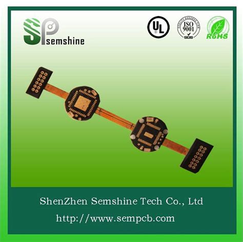
In the rapidly evolving world of electronics, the innovations in PCB assembly (PCBA) are pivotal in steering the technological advancements that define our modern experiences. As we delve into assembled circuit board technology, it’s clear that precision, efficiency, and smart integration stand at the forefront of this transformation.
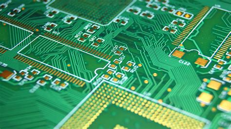
One of the most significant breakthroughs has been the use of nanotechnology in enhancing the electrical pathways within PCBs. This technology not only improves the conductivity but also increases the durability and lifespan of circuit boards. By incorporating nano-sized particles or layers into circuit board design, manufacturers are able to achieve a higher degree of miniaturization and complexity without compromising on performance.
Emerging trends in PCBA also include integrating smart materials which can adapt their properties under various conditions. These materials contribute to creating more resilient and adaptable electronic components. Alongside, advancements in automation have streamlined PCB assembly, making it faster and reducing human error.
“As we harness cutting-edge technologies like nanotechnology, smart materials, and automation, assembled circuit boards are becoming not just foundations but transformative elements within electronic devices.”
The integration of these technologies confirms that PCB assembly is not just about sticking components onto a board; it’s about enhancing every facet from material science to software integration. These innovations ensure that future devices will be more compact, efficient, environmentally friendly, and significantly more powerful. By focusing on these areas, we’re not only mastering current technologies but also paving the way for future developments that will continue to revolutionize our interaction with electronic devices.
Advancements in Smart Materials for Circuit Boards
In the evolving landscape of PCB assembly technology, the integration of smart materials is playing a pivotal role in enhancing the performance and durability of circuit boards. These materials respond dynamically to environmental stimuli such as temperature, pressure, or electrical signals, which contributes to the efficiency and adaptability of PCBA. For instance, the use of polymers that change conductivity based on different conditions can lead to significant energy savings and reduce wear and tear on the components.
Moreover, smart materials such as shape memory alloys (SMA) and piezoelectric materials are being increasingly incorporated into printed circuit boards. SMAs have the ability to return to their original shape after deformation when exposed to the appropriate heating conditions, which can be utilized in developing self-healing circuit boards. On the other hand, piezoelectric materials generate voltage when mechanically stressed. This property is used for creating advanced sensors that are embedded directly into PCBAs for monitoring structural health or environmental conditions.
These advancements not only improve the functionality of assembled circuit boards but also extend their lifespans and reduce maintenance frequency. By harnessing the properties of these smart materials, manufacturers are able to produce more reliable, robust, and technologically advanced electronic components. This not only boosts the overall performance but also offers enhanced flexibility in designing devices that are compact yet more powerful than their predecessors.
The innovative application of these smart materials signifies a transformative step towards modernizing PCB assembly with future-focused technologies that promise greater electrical efficiency and technological integration.
The Impact of Automation on Circuit Board Manufacturing
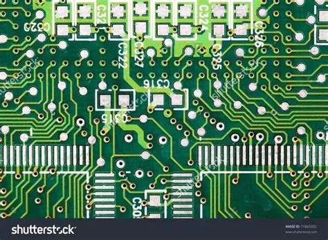
The integration of automation in PCB assembly processes has significantly transformed the landscape of electronics manufacturing. Through advanced robotics and computer systems, the assembly lines for PCB (Printed Circuit Board) components have become vastly more efficient and precise. Automation in PCBA (Printed Circuit Board Assembly) not only speeds up the production process but also reduces human error, contributing to higher quality end products.
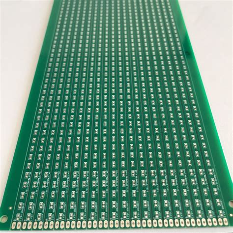
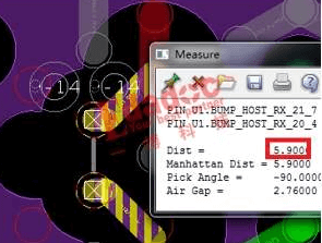
One of the pivotal benefits of automation is the ability to implement complex and precise component placements on circuit boards, which are crucial for the miniaturization trends in electronics. As devices continue to shrink, the demand for precise PCBA techniques increases. Automated systems are equipped with sophisticated sensors and imaging technologies that ensure components are accurately placed, even those that are nearly microscopic in size.
Moreover, automation facilitates seamless integration between different stages of the circuit board manufacturing process. From soldering to testing, automated systems provide a continuous flow that enhances production rates and ensures consistent quality across batches. This seamless operation is vital for meeting the growing demand for electronic devices in various industries, from consumer electronics to industrial applications.
Enhanced by AI technologies, automation also enables adaptive manufacturing techniques in circuit board production. These systems can learn from data generated during the manufacturing process and make real-time adjustments to improve efficiency and reduce waste. This not only optimizes resource use but also supports environmental sustainability by minimizing scrap material.
As we delve deeper into the future of technology, automated PCBA stands as a cornerstone that will drive innovation forward in electronic device production, ensuring that circuit boards are not only more efficient but also more capable of meeting advanced technological demands.
Trends in Miniaturization and Efficiency of Circuit Boards
The wave of miniaturization sweeping through the electronics industry is dramatically transforming the landscape of PCB assembly. As demands for smaller yet more powerful electronic devices continue to rise, engineers and developers are pushing the limits of what’s possible in PCB design. Emphasis on compact, energy-efficient solutions has led to significant advancements in the technology used for PCBA, where every millimeter counts and every joule is precious.
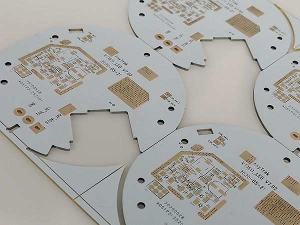
Central to these innovations is the use of advanced materials and sophisticated engineering techniques that allow for the reduction in size of circuit components while enhancing their functionality. The integration of high-density interconnect (HDI) technology is a prime example, supporting more complex circuits on a smaller board without compromising performance. This not only improves product aesthetics and consumer appeal but also significantly boosts functional capabilities.
Furthermore, developments in thermal management materials are critical as they help maintain efficiency and prolong the life of components packed closely together. Advances in conductive polymers, ceramics, and enhanced composite materials ensure that despite their reduced size, these circuit boards can handle the increased thermal loads that come with higher electrical demands.
The push towards greater efficiency also involves streamlining production processes through automation which ensures precision and reduces waste during PCB assembly. Enhanced accuracy in component placement and soldering through automated systems not only speeds up production but also minimizes errors that are more likely with manual processes, thereby increasing overall yield rates.
These breakthroughs are setting a new standard for how tomorrow’s electronic products are designed. By championing miniaturization and efficiency, the PCB industry is not merely adapting to current trends but actively shaping the future of global technology advancements.
Exploring the Integration of AI in Circuit Board Production
The integration of Artificial Intelligence (AI) in the field of PCB assembly is setting a new standard in the electronics industry. AI technologies are being leveraged to enhance the precision and speed of PCBA processes, significantly reducing human error and increasing productivity. Intelligent algorithms are now capable of analyzing complex PCB designs and recommending adjustments that optimize both the layout and functionality of the circuit board.
A notable innovation in this area is the use of machine learning models that predict and resolve potential assembly issues before they occur. These models are trained on vast datasets comprising various pcb assembly scenarios and their outcomes, enabling them to identify patterns that might lead to failure or inefficiencies. This preemptive approach not only saves valuable time and resources but also greatly improves the reliability of the final product.
Moreover, AI-driven automation tools are instrumental in streamlining component placement and soldering processes, which are crucial for achieving high-quality PCBA. These tools can adjust operations dynamically based on real-time feedback from the assembly line, ensuring optimal assembly conditions at all times.
The future implications of AI in PCB manufacturing are profound. As these technologies continue to evolve, they promise further advancements in miniaturization, efficiency, and functionality of assembled circuit boards. This revolution is not just enhancing current capabilities but is also paving the way for the next generation of electronic devices that are smarter, faster, and more efficient.
Future Prospects: The Next Generation of Electronic Devices
As we look to the horizon of electronic innovation, PCB assembly (PCBA) stands at the forefront of ushering in a new era of technological prowess. Advances in PCBA technology hint at future electronic devices that are not only more integrated but substantially more potent and energy-efficient. These enhancements are primarily driven by the relentless miniaturization and optimization of circuit components, enabling devices to perform more complex tasks without a corresponding increase in size or energy consumption.
A significant facet of this progression is the integration of smart materials into PCBAs, which adapt dynamically to environmental stimuli, offering unprecedented functionality and durability. Furthermore, the utilization of sophisticated automation techniques in PCB assembly lines is set to streamline production processes, reducing errors and increasing the speed of production without sacrificing quality.
Looking forward, we can anticipate that continuous innovations in nanotechnology will push the boundaries of what’s possible with PCBAs, making devices not just smaller, but smarter and more interconnected. This leap in capability promises to power a new generation of electronic devices that could seamlessly integrate with everyday life, enhancing personal and professional productivity.
In essence, as PCBA technology evolves, it paves the way for electronic devices that are comprehensive embodiments of efficiency and functionality. These advancements foster a landscape where electronics not only cater to current needs but are also well-equipped for future demands.
Conclusion
In our journey through the innovative landscape of assembled circuit board technology, we’ve seen compelling advances that underscore a promising future for electronics. The implementation of nanotechnology in enhancing PCB efficiency, alongside the integration of smart materials, has revolutionized the functionalities and capabilities of PCB assemblies. Furthermore, the surge in automation within PCBA production lines exemplifies how precision and speed can coexist, pushing productivity to new heights.
Emerging trends such as miniaturization have not only made circuit boards more compact but also significantly more powerful and energy-efficient. This leap in technology facilitates the development of smaller, yet more robust electronic devices that continue to reshape various industries. Additionally, the exploration into how artificial intelligence can be woven into PCBA processes is particularly exciting, offering predictions of self-optimizing manufacturing systems that could redefine industry standards.
As we look to the future, the evolution of PCB assembly points towards a landscape where electronic devices are not just tools, but collaborative partners in enhancing human endeavors across all facets of life. The continuous refinement and innovation in PCB assembly stand as a testament to the ingenuity and forward-thinking approach of engineers worldwide, promising an era where the interplay between technology and functionality reaches unprecedented levels.
FAQs
Frequently asked questions about innovations in PCB assembly serve as a crucial resource for understanding the complexities and advancements that shape today’s electronics. One common inquiry is about the role of nanotechnology in enhancing PCB effectiveness. By embedding nanoscale components, manufacturers are able to increase the functionality of printed circuit boards (PCBs) without increasing their size.
Another prevalent question pertains to how smart materials are influencing PCBA design. These materials adapt their properties under varying conditions, thereby optimizing performance and longevity of the electronics in which they are installed.
Prospective enhancements in PCBA automation also generate significant interest. Automation streamlines production and improves precision, thereby reducing human error and enhancing overall manufacturing efficiency.
The shift towards more compact and energy-efficient devices continues to guide innovation, leading to questions regarding the future capabilities and applications of miniaturized PCBs. This trend underscores advancements in both material science and digital technology, notably through AI integration, that push boundaries of what’s possible on a circuit board.
For more detailed insights into how these technologies could revolutionize your electronic products, ### please click here.