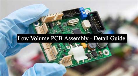
Maximizing Efficiency in Low-Volume PCB Assembly for Prototyping Success
Key Takeaways
Effective PCB assembly for low-volume prototyping hinges on balancing precision, speed, and cost-efficiency. By leveraging advanced PCBA techniques—such as automated pick-and-place systems and laser-cut stencils—teams can minimize human error while maintaining tight tolerances. Streamlined workflows often integrate design-for-manufacturability (DFM) principles, reducing iterative revisions and accelerating time-to-market.
A critical advantage of tailored low-volume PCB assembly lies in its adaptability. Flexible manufacturing processes enable rapid design validation, allowing engineers to test functional prototypes without overcommitting resources. To further optimize costs, consider modular component sourcing or panelization strategies that maximize material utilization.
Quality assurance remains non-negotiable, even in small batches. Implementing in-line inspection protocols—such as automated optical inspection (AOI) or X-ray testing—ensures reliability without compromising agility. Cost-effective scaling becomes achievable when PCBA workflows align with iterative prototyping needs, enabling seamless transitions from concept validation to pre-production phases.
By prioritizing these strategies, teams can transform PCB assembly from a logistical hurdle into a catalyst for innovation, ensuring that every prototype iteration drives meaningful progress toward final product readiness.
Low-Volume PCB Assembly Precision Techniques
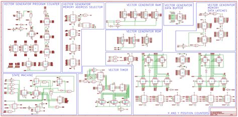
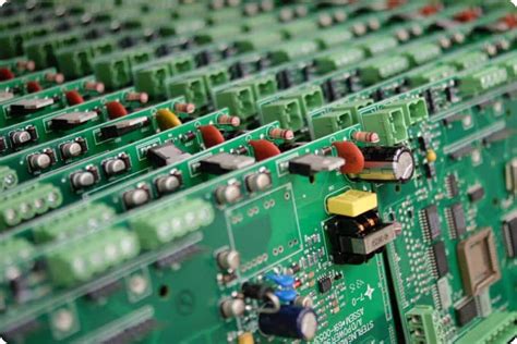
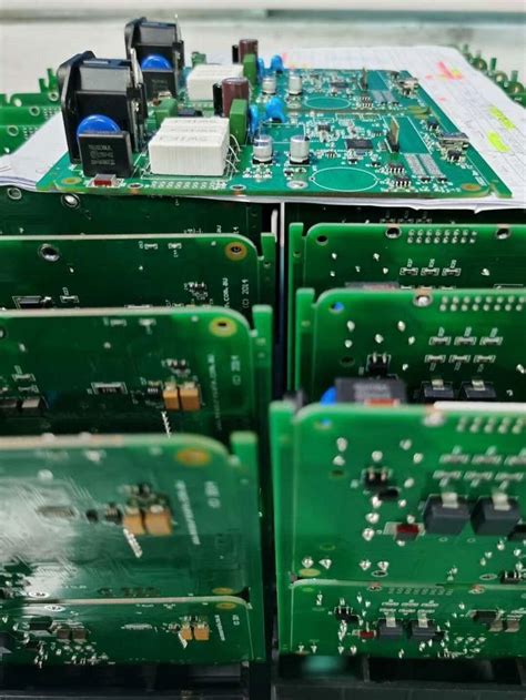
Achieving precision in low-volume PCB assembly requires a combination of advanced equipment, meticulous process control, and specialized expertise. For prototyping applications, even minor deviations in component placement or soldering can compromise functionality, making precision techniques indispensable. Modern PCBA workflows leverage automated optical inspection (AOI) systems to detect microscopic defects, while laser-cut stencils ensure consistent solder paste application for fine-pitch components. Design-for-manufacturability (DFM) principles further enhance accuracy by aligning board layouts with assembly capabilities, reducing rework risks.
| Technique | Application | Impact on Precision |
|---|---|---|
| AOI Systems | Defect detection | ±0.01mm measurement accuracy |
| Laser Stenciling | Solder paste deposition | 99.9% consistency in paste volume |
| Micro-SMT Placement | Miniaturized components | 01005 component handling |
To maintain reliability in low-volume PCB assembly, manufacturers often employ statistical process control (SPC) to monitor critical parameters like soldering temperatures and placement pressure. This data-driven approach minimizes variability, particularly for high-density interconnect (HDI) designs common in IoT and medical devices. Additionally, selective soldering systems enable precise targeting of through-hole components without affecting adjacent surface-mount parts. By integrating these strategies, teams can balance speed and accuracy, ensuring prototypes meet functional requirements while laying the groundwork for scalable PCBA processes. Such precision not only accelerates validation cycles but also reduces costly iterations, aligning with the broader goal of optimizing prototyping efficiency.
Streamline Prototyping Workflows Efficiently
Effective PCB assembly for prototyping requires balancing speed, precision, and flexibility. By adopting design standardization practices, engineers can minimize rework during low-volume PCBA processes. For instance, leveraging modular component libraries reduces time spent on schematic adjustments, while automated design-for-manufacturability (DFM) checks identify potential conflicts early. Integrating just-in-time material sourcing with trusted suppliers further eliminates delays caused by part shortages or obsolete inventory.
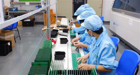
To enhance workflow efficiency, consider implementing batch processing for similar prototype iterations. This approach allows manufacturers to group orders with overlapping specifications, optimizing machine setup times without compromising customization. Advanced PCB assembly tools, such as programmable pick-and-place systems, enable rapid transitions between projects, ensuring consistent quality across diverse prototypes.
Additionally, real-time collaboration between design and production teams is critical. Cloud-based platforms provide instant feedback loops, allowing engineers to refine layouts based on manufacturability insights before initiating PCBA. Pairing this with automated optical inspection (AOI) systems ensures defects are caught early, reducing costly revisions. By aligning these strategies, teams can accelerate prototyping cycles while maintaining the agility needed for iterative innovation.
Cost-Effective Strategies for PCB Prototyping
Achieving cost efficiency in PCB assembly for prototyping requires a balanced approach that prioritizes both technical precision and budget optimization. One effective method involves leveraging design simplification to minimize component complexity, reducing material waste and assembly time. By collaborating with PCBA providers specializing in low-volume production, engineers gain access to scalable pricing models tailored for iterative development.
Tip: Always request a Design for Manufacturability (DFM) review early in the prototyping phase. This step identifies potential cost drivers, such as oversized boards or non-standard components, before they impact your budget.
Adopting panelization techniques—grouping multiple prototypes onto a single panel—can further lower per-unit costs in PCB assembly while maintaining quality. Additionally, opting for standardized surface finishes like HASL (Hot Air Solder Leveling) instead of premium alternatives ensures reliable performance without unnecessary expenses. For components, consider using reel-to-reel packaging for automated placement in PCBA workflows, which streamlines assembly and reduces manual labor costs.
Strategic supplier partnerships also play a critical role. Suppliers offering bundled services—such as prototyping-friendly PCB assembly and component sourcing—eliminate markup layers, ensuring transparency in pricing. Finally, modular design practices enable reuse of validated subcircuits across iterations, accelerating development while preserving cost efficiency.
Accelerate Development Cycles with Tailored Assembly
Tailored PCB assembly strategies play a pivotal role in accelerating product development, particularly for prototyping phases where time-to-market is critical. By prioritizing agility and precision in low-volume PCBA, engineers can swiftly iterate designs without compromising functionality. Customized workflows, such as just-in-time component sourcing and modular assembly techniques, eliminate bottlenecks inherent in traditional manufacturing. For instance, partnering with a PCBA provider that offers flexible batch sizes ensures rapid turnaround for design validation, enabling teams to test multiple iterations within compressed timelines.
A key advantage lies in optimizing supply chain coordination. By leveraging pre-validated component libraries and automated assembly processes, manufacturers reduce lead times while maintaining consistency. This approach not only accelerates prototyping but also minimizes costly redesigns by identifying potential flaws early. Additionally, integrating design-for-assembly (DFA) principles ensures compatibility between schematics and manufacturing capabilities, further streamlining transitions from prototype to scaled production.
To maximize efficiency, consider hybrid models that combine PCB assembly automation with manual oversight for complex configurations. This balance allows for high-mix, low-volume adaptability while preserving quality. By aligning assembly methodologies with project-specific requirements, teams can shave weeks off development cycles, ensuring innovations reach validation stages faster without sacrificing reliability.
Optimizing PCB Assembly for Rapid Innovation
Achieving rapid innovation in electronics development hinges on refining PCB assembly processes to balance speed and precision. Unlike traditional high-volume production, low-volume PCBA requires adaptable strategies that accommodate frequent design changes without compromising quality. Implementing automated optical inspection (AOI) systems early in the assembly line ensures defects are identified at nascent stages, reducing rework delays. Additionally, leveraging modular design principles allows engineers to isolate functional blocks, simplifying updates during iterative prototyping.
A critical focus lies in optimizing component sourcing for low-volume runs. Partnering with suppliers offering just-in-time inventory minimizes lead times while maintaining access to specialized parts. Advanced PCB assembly techniques, such as laser-depaneling and selective soldering, further accelerate turnaround by eliminating manual steps. For instance, integrating design-for-manufacturability (DFM) feedback loops between engineers and PCBA providers ensures layouts are inherently optimized for assembly, reducing post-production adjustments.
Finally, adopting agile workflows—like parallel testing and concurrent engineering—enables teams to validate prototypes while refining subsequent iterations. This approach not only shortens development cycles but also aligns with cost-effective scaling strategies discussed earlier in the article. By harmonizing these methods, innovators can transform PCB assembly from a bottleneck into a catalyst for breakthroughs.
Implementing Quality Control in Low-Volume Production
Maintaining rigorous quality control (QC) in low-volume PCB assembly is critical to ensuring prototyping success, even when manufacturing at smaller scales. Unlike high-volume production, low-volume PCBA runs demand adaptable inspection protocols that balance precision with efficiency. Automated Optical Inspection (AOI) and X-ray testing remain foundational, but their application must be optimized for smaller batches to avoid unnecessary delays. For instance, statistical process control (SPC) tools can be calibrated to track fewer units while still identifying deviations in solder joint integrity or component placement.
A key challenge lies in preserving consistency across prototypes, particularly when design iterations occur rapidly. Implementing traceability systems — such as barcoding or laser marking — ensures each PCB assembly can be tracked through testing phases, simplifying root-cause analysis if defects emerge. Additionally, integrating Design-for-Manufacturability (DFM) feedback loops early in prototyping helps preempt quality issues, reducing rework cycles.
Transitioning seamlessly from design to production requires collaboration between engineering and assembly teams. By adopting risk-based testing strategies, manufacturers can prioritize critical inspection points without overburdening workflows. This approach not only safeguards reliability but also aligns with cost-effective PCBA practices, ensuring that quality assurance remains a driver of innovation rather than a bottleneck.
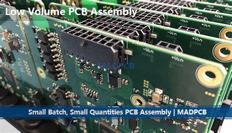
Scaling Prototyping Success via Efficient Assembly
Achieving scalable prototyping outcomes hinges on optimizing PCB assembly workflows to align with the unique demands of low-volume production. By leveraging advanced PCBA techniques, engineers can strike a balance between precision and agility, ensuring prototypes meet functional requirements without compromising development timelines. A critical step involves adopting design-for-manufacturability (DFM) principles early in the process, which minimizes rework by tailoring layouts for efficient component placement and soldering. For instance, using modular designs or standardized footprints accelerates assembly while reducing material waste.
Automation plays a pivotal role in streamlining low-volume PCB assembly, particularly for tasks like solder paste application and component placement. Modern pick-and-place systems, paired with automated optical inspection (AOI), enhance accuracy and repeatability even for complex boards. Integrating real-time data tracking further refines workflows, enabling teams to identify bottlenecks in PCBA processes and adjust resource allocation dynamically.
Cost efficiency remains central to scaling success. By consolidating orders or utilizing just-in-time inventory strategies, businesses can mitigate expenses associated with small-batch PCB assembly without sacrificing quality. Collaborative partnerships with specialized manufacturers also ensure access to expertise in handling niche materials or high-mix configurations. Ultimately, these strategies create a foundation for rapid iteration, allowing innovators to refine prototypes faster and transition seamlessly to full-scale production.
Reducing Costs in Low-Volume Electronic Prototyping
Effective cost management in low-volume PCB assembly begins with strategic component sourcing and design optimization. By leveraging standardized parts and avoiding over-specification, engineers can reduce material expenses without compromising functionality. For instance, selecting PCBA-compatible components from verified suppliers minimizes procurement delays and ensures compatibility with automated assembly processes. Additionally, early-stage design reviews help identify potential inefficiencies, such as unnecessary layers or complex routing, which inflate production costs in small batches.
Adopting modular design principles further streamlines prototyping. Breaking circuits into reusable blocks allows teams to test individual modules before full-system integration, reducing rework and material waste. Partnering with PCB assembly specialists who offer flexible pricing models—such as volume-tiered discounts or shared panelization—can also lower per-unit costs. Advanced PCBA technologies, like surface-mount device (SMD) placement, enhance precision while shortening turnaround times, directly impacting development budgets.
Finally, integrating prototype-specific testing protocols ensures defects are caught early, avoiding costly post-production fixes. By balancing low-volume PCB assembly efficiencies with rigorous quality checks, teams achieve cost-effective prototyping that aligns with rapid innovation goals.
Conclusion
In the realm of electronic prototyping, low-volume PCB assembly serves as the backbone for transforming conceptual designs into functional innovations. By integrating precision techniques and tailored workflows, manufacturers can strike a balance between speed, cost, and quality—even in small-batch production. The strategic adoption of PCBA processes not only accelerates development cycles but also ensures that prototypes meet rigorous performance standards, laying a foundation for scalable success.
Key to this approach is the alignment of PCB assembly methodologies with prototyping goals. Iterative testing and modular design principles enable engineers to identify flaws early, reducing costly revisions. Furthermore, leveraging automated tools for PCBA tasks—such as solder paste application and component placement—enhances consistency while minimizing human error.
Ultimately, the value of optimizing low-volume PCB assembly lies in its ability to bridge the gap between innovation and market readiness. By prioritizing agile manufacturing and robust quality checks, teams can mitigate risks, control expenses, and deliver prototypes that align with both technical specifications and business objectives. This focus on efficiency ensures that even limited production runs contribute meaningfully to the broader product development lifecycle.
FAQs
How does low-volume PCB assembly differ from mass production?
Low-volume PCBA focuses on precision and flexibility, prioritizing rapid iteration over scale. This approach allows engineers to test critical design elements before committing to full-scale manufacturing, reducing risks in early prototyping phases.
What cost factors should be considered in low-volume PCB assembly?
Key expenses include material selection, component sourcing, and setup fees. Optimizing PCBA workflows through panelization and standardized design rules can lower per-unit costs while maintaining prototyping integrity.
How can quality control be ensured in small-batch PCB assembly?
Automated optical inspection (AOI) and functional testing protocols are essential. Reputable providers combine these with traceability systems to identify defects early, ensuring reliability even in low-volume production runs.
What turnaround times are realistic for prototype PCB assembly?
Advanced PCBA services typically deliver prototypes within 5-10 days, depending on design complexity. Expedited options using pre-certified components can further accelerate development cycles without compromising testing rigor.
Can low-volume PCB assembly support scaling to mass production?
Yes, modular PCBA processes allow seamless transition to higher volumes. Prototype-phase documentation and validated assembly methods create reproducible workflows, minimizing rework during scaling.
Optimize Your Next Prototype Project
For tailored PCB assembly solutions balancing speed and precision, please click here to explore specialized PCBA services designed for prototyping excellence.