Maximizing Efficiency in PCB OEM Manufacturing Processes

Key Takeaways
Effective PCB OEM manufacturing relies on balancing workflow optimization, material utilization, and automated quality control to achieve cost and time savings. Central to these improvements is the integration of smart manufacturing principles, which enable real-time adjustments across pcb assembly lines. For instance, deploying automated optical inspection (AOI) systems during pcba stages reduces human error by 40–60%, while predictive analytics tools optimize material procurement, trimming waste by up to 25%.
| Aspect | Traditional Approach | Optimized Strategy |
|---|---|---|
| Quality Assurance | Manual visual checks | AOI-enabled defect detection |
| Material Management | Fixed inventory models | AI-driven demand forecasting |
| Lead Time Reduction | Sequential production stages | Parallelized pcb assembly workflows |
Adopting data-driven decision-making ensures continuous improvement, with metrics like first-pass yield and equipment uptime guiding refinements. Additionally, aligning design for manufacturing (DFM) principles with pcba requirements minimizes rework, accelerating time-to-market. These strategies collectively address cost-reduction and sustainability, positioning manufacturers to adapt to evolving demands in PCB OEM ecosystems. As the foundation for subsequent sections, these takeaways underscore the importance of integrating innovation at every production phase.

Optimizing PCB OEM Workflow Efficiency
Effective workflow optimization in PCB OEM manufacturing begins with analyzing value streams to eliminate bottlenecks in PCB assembly processes. Implementing lean manufacturing principles, such as standardized work instructions and parallel task sequencing, reduces idle time between PCBA stages. Advanced planning systems that synchronize component procurement with production schedules can shorten cycle times by up to 30%, particularly when integrated with automated surface-mount technology (SMT) lines.
Tip: Conduct time-motion studies quarterly to identify recurring delays in solder paste application or pick-and-place operations.
Digital twin simulations enable manufacturers to test layout adjustments virtually before physical reconfiguration, minimizing downtime during workflow transitions. For PCB assembly lines, integrating enterprise resource planning (ERP) with manufacturing execution systems (MES) ensures real-time visibility into material availability and equipment utilization. A case study from Tier-1 OEMs shows that automating documentation workflows for PCBA testing reduced administrative overhead by 22% while improving compliance tracking accuracy.
Critical to this optimization is fostering cross-department collaboration. Engineering teams should perform design for manufacturability (DFM) checks during prototyping to avoid rework in later stages. Meanwhile, adaptive scheduling algorithms can dynamically reroute batches during unexpected downtime, maintaining throughput even in high-mix production environments. By aligning these strategies, manufacturers achieve a 15–25% improvement in overall equipment effectiveness (OEE) across PCB OEM operations.
PCB Material Usage Optimization Strategies
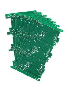
Effective material management forms the backbone of cost-efficient PCB assembly processes. By adopting data-driven design practices, manufacturers can minimize waste while maintaining performance standards. For instance, optimizing panelization layouts reduces PCBA substrate scrap by up to 18%, directly lowering raw material costs. Advanced nesting algorithms further enhance material utilization rates, ensuring maximum yield from copper-clad laminates and prepreg sheets.
Strategic material selection also plays a pivotal role. Transitioning to high-performance substrates with tighter tolerance ranges reduces rework during PCB assembly, while standardized material inventories streamline procurement for recurring PCBA projects. Implementing just-in-time inventory systems mitigates overstocking risks, particularly for specialty materials like high-frequency laminates.
Additionally, integrating design-for-manufacturing (DFM) principles early in the development cycle prevents material-intensive redesigns. Collaborative tools that synchronize CAD data with PCB assembly capabilities enable engineers to balance electrical requirements with material efficiency. For example, adjusting trace widths or via placements can conserve copper usage without compromising signal integrity.
Emerging technologies like AI-powered predictive analytics further refine material strategies by forecasting demand fluctuations and identifying underutilized material alternatives. These innovations, combined with real-time monitoring of PCBA production lines, create a closed-loop system for continuous material optimization.
Automated Quality Control in PCB Manufacturing
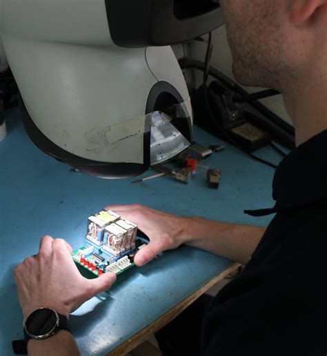
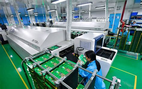
Modern PCB assembly processes increasingly rely on automated quality control systems to ensure precision while minimizing human error. Advanced optical inspection (AOI) tools, combined with AI-powered defect recognition algorithms, enable real-time detection of issues such as misaligned components, solder bridging, or trace defects during PCBA stages. These systems analyze thousands of points per board at speeds unattainable through manual inspection, reducing rework rates by up to 40% in high-volume production.
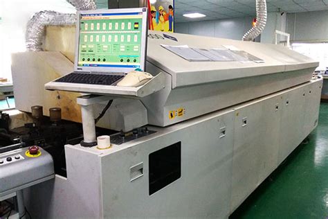
Integration with machine vision and X-ray inspection further enhances reliability for multilayer or high-density designs, where hidden flaws in vias or internal layers could compromise performance. Automated workflows also synchronize with enterprise resource planning (ERP) systems, creating closed-loop feedback for continuous process optimization. For instance, data from PCB assembly lines can trigger adjustments in solder paste application or reflow oven profiles, preventing recurring defects.
The shift toward smart manufacturing in PCBA extends to predictive maintenance, where sensor-equipped machinery anticipates equipment wear before it impacts quality. This proactive approach not only sustains yield rates but also aligns with lean manufacturing principles by eliminating downtime. By embedding quality checks at every stage—from bare board testing to final functional validation—manufacturers achieve zero-defect manufacturing targets while maintaining compliance with industry standards like IPC-A-610.
Cost-Reduction Techniques for OEM PCB Production
Implementing cost-saving measures in PCB assembly requires a holistic approach that balances quality with financial efficiency. One proven method involves optimizing design-for-manufacturability (DFM) principles, which minimize material waste and reduce rework by aligning circuit layouts with production capabilities. By leveraging advanced PCBA simulation tools, engineers can identify potential defects early, preventing costly post-production fixes. Additionally, adopting standardized component libraries streamlines procurement, lowering inventory costs while maintaining compatibility across projects.
Strategic supplier partnerships further enhance savings through bulk purchasing agreements and negotiated lead times for critical materials like high-frequency laminates or solder masks. For instance, consolidating orders for multilayer boards across multiple projects often unlocks volume pricing advantages. Automation also plays a pivotal role: robotic soldering systems and AI-driven pick-and-place machines accelerate PCB assembly throughput while reducing labor expenses. Energy-efficient reflow ovens and modular production lines further cut operational costs by minimizing power consumption and downtime during retooling.
To maintain competitiveness, manufacturers are increasingly integrating real-time analytics into PCBA workflows. Monitoring metrics like yield rates and cycle times enables data-driven adjustments, ensuring resources are allocated to high-margin processes. Combined with lean manufacturing principles, these techniques create a scalable framework for cost reduction without compromising the reliability of end products.
Accelerating Lead Times in PCB Manufacturing
Reducing production timelines in PCB assembly requires coordinated efforts across design, procurement, and manufacturing stages. Implementing design for manufacturing (DFM) principles early in the product development cycle minimizes revisions by aligning component placement and routing with PCBA capabilities. Advanced planning tools enable real-time material tracking, ensuring critical components arrive just-in-time to avoid bottlenecks. Automated optical inspection (AOI) systems further streamline workflows by identifying defects during PCB assembly, reducing rework cycles by up to 30%.
Optimized panelization strategies maximize substrate utilization while maintaining compatibility with high-speed PCBA equipment. Modular production lines, combined with dynamic scheduling algorithms, allow rapid switching between batches without sacrificing precision. For time-sensitive projects, parallel processing of prototyping and testing phases accelerates validation, particularly when integrating complex multilayer designs. Collaborative platforms linking OEMs with suppliers also enhance transparency, enabling proactive adjustments to material shortages or design changes.
By adopting these practices, manufacturers can compress lead times by 15–25% while maintaining stringent quality standards—a critical advantage in industries where time-to-market dictates competitive success.
Smart Manufacturing Integration for PCB OEM
The adoption of smart manufacturing technologies is revolutionizing PCB assembly workflows, enabling OEMs to achieve unprecedented levels of precision and scalability. By integrating IoT-enabled devices and AI-driven analytics, manufacturers can monitor PCBA production lines in real time, identifying bottlenecks and optimizing resource allocation. Advanced machine learning algorithms analyze historical data to predict equipment maintenance needs, reducing unplanned downtime by up to 30%.
Central to this transformation is the implementation of digital twin simulations, which create virtual replicas of physical assembly processes. These models allow engineers to test design iterations and process adjustments without disrupting active production, accelerating time-to-market for complex PCB assembly projects. Additionally, automated optical inspection (AOI) systems equipped with computer vision enhance defect detection accuracy, ensuring consistent quality across high-volume PCBA orders.
To further streamline operations, cloud-based enterprise resource planning (ERP) systems synchronize procurement, inventory management, and production scheduling. This interconnected approach minimizes material waste and ensures just-in-time component delivery, aligning with lean manufacturing principles. As smart factories evolve, the integration of 5G connectivity and edge computing will enable faster data processing, empowering OEMs to adapt dynamically to shifting market demands while maintaining cost-efficiency.
Sustainable Practices in PCB OEM Processes
Adopting sustainable practices in PCB OEM manufacturing not only aligns with global environmental goals but also enhances long-term operational efficiency. A critical focus lies in optimizing material selection—for instance, using lead-free solders and halogen-free substrates—to reduce hazardous waste during PCB assembly. Manufacturers are increasingly integrating closed-loop recycling systems to reclaim metals like copper from production scrap, minimizing raw material consumption. Energy-efficient equipment, such as low-power soldering irons and reflow ovens, further reduces the carbon footprint of PCBA processes.
Another key strategy involves streamlining workflows to cut energy waste. Automated optical inspection (AOI) systems, while ensuring precision in PCB assembly, also reduce rework rates, lowering energy and material usage. Additionally, adopting lean manufacturing principles helps eliminate excess inventory and overproduction, which are common sources of waste in OEM PCB production.
To strengthen sustainability, many OEMs now prioritize suppliers with certified eco-friendly materials and enforce compliance with standards like ISO 14001 and RoHS. By embedding these practices into PCBA workflows, manufacturers achieve cost savings through reduced waste penalties and energy bills while meeting rising demand for greener electronics. This holistic approach ensures environmental responsibility without compromising production scalability or quality.

Data-Driven Process Improvements in PCB OEM
Modern PCB OEM operations increasingly rely on data analytics to refine manufacturing precision and operational agility. By integrating PCB assembly line sensors with advanced analytics platforms, manufacturers gain real-time visibility into parameters like solder paste deposition accuracy, component placement rates, and reflow oven temperature profiles. This granular data enables predictive maintenance models, reducing unplanned downtime by 18-25% in PCBA workflows. Machine learning algorithms further optimize material consumption by correlating design complexity with substrate waste patterns, achieving up to 12% improvement in copper laminate utilization.
Transitioning from reactive to proactive quality management, statistical process control (SPC) tools analyze defect trends across PCB assembly batches, allowing engineers to adjust tolerances before critical failures occur. For instance, thermal profiling data from infrared cameras helps fine-tune reflow soldering parameters, minimizing void formation in high-density interconnects. These insights also feed backward into design-for-manufacturability (DFM) guidelines, closing the loop between production feedback and future PCBA design iterations. As IoT-enabled devices proliferate in smart factories, the fusion of edge computing and centralized data lakes ensures scalability for multi-site PCB OEM networks, aligning with broader Industry 4.0 adoption trends while maintaining compliance with evolving sustainability benchmarks.
Conclusion
The evolution of PCB OEM manufacturing underscores the critical balance between precision, speed, and cost-effectiveness. By integrating automated quality control systems with data-driven process optimization, manufacturers can achieve unprecedented consistency in PCBA outputs while minimizing waste. The adoption of smart manufacturing principles—such as IoT-enabled monitoring and predictive maintenance—further strengthens production resilience, particularly in high-volume PCB assembly environments.
Equally vital is the strategic alignment of material utilization practices with lean manufacturing frameworks, which not only reduces overhead but also supports sustainable operations. As demonstrated, advancements in rapid prototyping and supply chain digitization directly contribute to compressed lead times without compromising on reliability. For OEMs, the convergence of these strategies creates a competitive edge, enabling faster response to market demands while maintaining stringent quality benchmarks.
Ultimately, the future of PCB OEM success hinges on continuous innovation, where real-time analytics and cross-functional collaboration become standard pillars of production ecosystems. By prioritizing both technological agility and operational transparency, manufacturers can sustainably meet the dual imperatives of cost efficiency and performance excellence in an increasingly dynamic industry.
Frequently Asked Questions
How does automated quality control improve reliability in PCB assembly?
Advanced systems like automated optical inspection (AOI) and X-ray inspection minimize human error by detecting defects in PCBA at micron-level precision. These tools ensure consistent adherence to IPC-A-610 standards while reducing rework rates by up to 40%.
What strategies optimize material usage for high-volume PCB assembly?
Implementing design for manufacturability (DFM) principles and panelization techniques maximizes substrate utilization. For PCBA, standardized component libraries and reel optimization reduce waste, achieving material efficiency gains of 15–25% in typical production runs.
Can smart manufacturing reduce lead times for complex PCBA projects?
Yes. Integration of IoT-enabled production tracking and AI-driven demand forecasting slashes lead times by synchronizing material procurement with assembly workflows. This reduces idle time between PCB fabrication and PCBA stages by 30–50%.
How do sustainable practices impact PCB assembly costs?
Adopting lead-free finishes and recyclable substrates lowers compliance risks and waste disposal fees. Energy-efficient soldering processes in PCBA further cut operational costs by 12–18% while meeting global environmental regulations.
What role does data analytics play in PCBA quality assurance?
Real-time analytics from automated test equipment (ATE) identify process deviations before defects occur. By correlating PCBA failure patterns with machine parameters, manufacturers achieve first-pass yield improvements exceeding 20%.
Ready to Optimize Your PCB Assembly Process?
For tailored solutions in high-efficiency PCBA manufacturing, please click here to explore our advanced PCB assembly services.