Maximizing Production Efficiency with Precision PCBA Service Integration

Key Takeaways
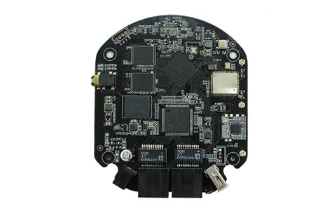
Implementing PCBA (Printed Circuit Board Assembly) services into manufacturing workflows drives operational excellence by unifying design, assembly, and testing phases. Precision engineering in PCB assembly ensures components are placed with micron-level accuracy, reducing rework and material waste. For instance, automated pick-and-place systems paired with solder paste inspection (SPI) tools achieve error rates below 0.1%, directly enhancing production efficiency.
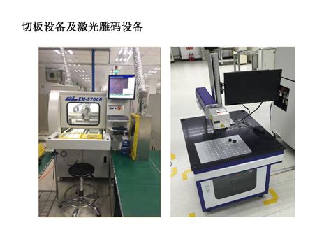
A critical advantage lies in rigorous testing protocols, such as automated optical inspection (AOI) and in-circuit testing (ICT), which identify defects early in the cycle. This proactive approach minimizes costly post-production corrections. Consider the table below, which contrasts traditional vs. integrated PCBA strategies:
| Aspect | Traditional Approach | Integrated PCBA |
|---|---|---|
| Assembly Time | 8-10 days | 4-6 days |
| Error Rate | 2-3% | <0.5% |
| Scalability | Limited batch sizes | Flexible volume adjustments |
Moreover, scalable solutions enable seamless transitions from prototyping to mass production, aligning with fluctuating market demands. By integrating PCBA workflows with enterprise resource planning (ERP) systems, manufacturers gain real-time visibility into inventory and throughput, accelerating time-to-market by up to 30%. These synergies underscore how modern PCB assembly services act as catalysts for lean, agile operations.
Precision PCBA Services Boost Production Efficiency
Modern manufacturing demands require PCBA providers to deliver speed without compromising quality. By integrating advanced PCB assembly techniques, precision-focused services minimize material waste and reduce rework cycles. Automated pick-and-place systems, combined with optical inspection tools, ensure component placement accuracy to within microns—critical for high-density boards. Real-time monitoring of solder paste application and reflow profiles further optimizes process consistency, directly enhancing throughput.
Tip: For complex projects, prioritize vendors offering traceable process documentation. This simplifies root-cause analysis if post-assembly defects occur.
The synergy between PCBA design validation and production planning also plays a pivotal role. Early collaboration with engineering teams allows for Design for Manufacturability (DFM) adjustments, preventing costly mid-production redesigns. Rigorous pre-production prototyping identifies potential thermal or signal integrity issues, ensuring seamless scaling to full-volume runs. Additionally, modular manufacturing workflows enable rapid transitions between low- and high-mix batches, aligning output with fluctuating market demands.
By embedding quality control at every stage—from solder mask alignment to final functional testing—precision-driven PCB assembly services achieve first-pass yield rates exceeding 98% in optimized setups. This systematic approach not only accelerates timelines but also reduces resource expenditure, making it indispensable for industries requiring both precision and scalability.
Streamlining Electronics Assembly with PCBA Solutions
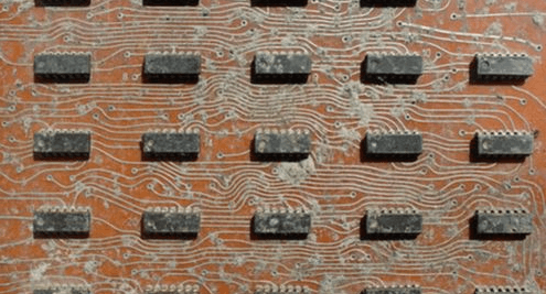
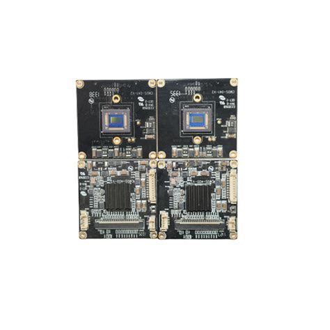
Modern PCB assembly processes rely on integrated PCBA solutions to eliminate bottlenecks in electronics manufacturing. By combining automated component placement systems with precision soldering technologies, manufacturers achieve consistent first-pass yields while reducing manual intervention. Advanced PCBA workflows leverage surface-mount technology (SMT) for high-density layouts, paired with automated optical inspection (AOI) to validate solder joint integrity in real time. This harmonized approach minimizes rework cycles, particularly when handling complex designs such as mixed-technology boards or fine-pitch ICs.
A critical advantage lies in the modularity of contemporary PCB assembly systems, which allow rapid reconfiguration for diverse product batches. For instance, flexible manufacturing cells enable seamless transitions between prototyping and full-scale production without compromising throughput. This scalability proves vital for industries facing fluctuating demand, from IoT device makers to automotive electronics suppliers. By synchronizing design-for-manufacturing (DFM) principles with PCBA execution, engineers preemptively address thermal management and signal integrity challenges, ensuring assemblies meet mission-critical reliability standards. Such integration not only accelerates production timelines but also creates a foundation for implementing Industry 4.0 data analytics across the assembly lifecycle.
Rigorous Testing Protocols Minimize Manufacturing Errors
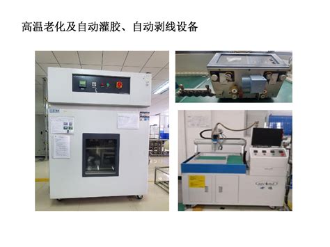
Modern PCBA (Printed Circuit Board Assembly) processes rely on rigorous testing protocols to identify and eliminate defects at critical production stages. Automated Optical Inspection (AOI) systems scan solder joints and component placements with micron-level accuracy, while X-ray inspection verifies hidden connections in Ball Grid Array (BGA) packages. Functional testing replicates real-world operating conditions to validate board performance, and In-Circuit Testing (ICT) probes electrical characteristics to pinpoint manufacturing deviations. By implementing these multi-layered checks, PCB assembly providers reduce error rates by up to 98% compared to manual verification methods, according to industry benchmarks. Advanced testing workflows also integrate with design-for-manufacturability (DFM) principles, enabling engineers to address potential failure points during prototyping. This proactive approach minimizes rework cycles and prevents costly recalls, ensuring compliance with automotive and medical-grade reliability standards. As a result, manufacturers achieve higher first-pass yields while maintaining consistent quality across high-volume production runs.
Scalable PCBA Strategies Accelerate Time-to-Market
Implementing scalable PCBA strategies enables manufacturers to adapt swiftly to fluctuating market demands without compromising quality. By leveraging modular PCB assembly workflows, companies can dynamically adjust production volumes—whether prototyping low batches or ramping up for high-volume orders. This agility is critical in industries where time-to-market directly impacts competitive advantage, such as consumer electronics or IoT devices.
Advanced PCBA service providers achieve scalability through standardized processes, including automated component placement and cloud-based inventory management. These systems minimize manual intervention, reducing bottlenecks during peak production cycles. For instance, integrating flexible manufacturing lines ensures seamless transitions between product iterations, cutting lead times by up to 30% in multi-phase projects.
Moreover, scalable solutions prioritize design-for-manufacturability (DFM) principles, aligning PCB assembly requirements with end-to-end production capabilities. By embedding test points and optimizing panel layouts early in the design phase, teams avoid costly rework during scaling. Real-time data analytics further enhance decision-making, enabling proactive adjustments to material sourcing or throughput rates.
Ultimately, the synergy between adaptable PCBA infrastructures and strategic planning empowers businesses to meet deadlines consistently while maintaining precision across all manufacturing stages.
Integrated Workflows Enhance PCB Assembly Accuracy
Modern PCBA solutions thrive on seamless integration across design, fabrication, and testing phases. By unifying these stages into cohesive workflows, manufacturers minimize gaps that traditionally lead to miscommunication or component mismatches. For instance, automated design-to-production pipelines enable real-time adjustments, ensuring PCB assembly aligns precisely with engineering specifications. Advanced software tools synchronize bill-of-materials (BOM) updates with assembly line configurations, reducing manual intervention and human error.
A critical advantage lies in the synchronization of PCBA testing protocols with assembly processes. Inline inspection systems, such as automated optical inspection (AOI), immediately flag deviations during solder paste application or component placement. This closed-loop feedback allows corrections before defects propagate downstream, preserving both accuracy and yield rates. Additionally, integrated workflows leverage machine learning algorithms to predict potential bottlenecks, optimizing material flow and equipment calibration for consistent output.
Scalability further benefits from this holistic approach. Modular PCB assembly systems adapt dynamically to varying production volumes without compromising precision. By embedding quality checks at every stage—from solder paste deposition to final functional testing—manufacturers achieve near-zero defect rates while maintaining agility. Such integration not only elevates accuracy but also reinforces the reliability of PCBA outputs, ensuring products meet stringent industry standards and end-user expectations.
Error-Reduction Tactics in Modern PCBA Processes
Modern PCB assembly workflows prioritize minimizing defects through advanced error-reduction strategies. By integrating automated optical inspection (AOI) systems, PCBA providers can detect microscopic soldering flaws or misaligned components in real time, reducing human oversight. Machine learning algorithms further enhance defect prediction by analyzing historical production data to identify high-risk patterns before they escalate. For instance, solder paste inspection (SPI) tools ensure precise deposition volumes, mitigating risks like bridging or insufficient joints.
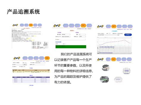
Another critical tactic involves adopting standardized design-for-manufacturing (DFM) guidelines. Collaborating early with PCBA engineers allows designers to address potential thermal mismanagement or signal integrity issues, streamlining the transition from prototyping to mass production. Additionally, traceability systems embedded in PCB assembly lines track each component’s lifecycle, enabling rapid root-cause analysis if anomalies arise. These measures not only align with rigorous testing protocols but also reinforce the scalability of manufacturing workflows. By combining predictive analytics with closed-loop feedback mechanisms, manufacturers achieve tighter process control, ensuring consistent quality across high-volume orders.
Optimized PCBA Solutions for Mass Production Demands
Meeting high-volume manufacturing requirements demands PCBA strategies that prioritize both speed and consistency. By leveraging automated PCB assembly workflows, manufacturers can achieve repeatable precision across thousands of units while minimizing human intervention. Advanced pick-and-place systems, coupled with solder paste inspection (SPI) technologies, ensure component placement accuracy down to micrometer-level tolerances, a critical factor for industries like automotive or IoT devices where reliability is non-negotiable.
Scalability is further enhanced through modular production line designs, which allow rapid reconfiguration for different product batches without compromising throughput. For example, integrated PCBA service providers often employ dual-track conveyor systems to parallelize tasks such as soldering and optical inspection, effectively reducing cycle times by 15–20%. Real-time data analytics also play a pivotal role, enabling predictive maintenance of assembly equipment to prevent unplanned downtime during extended production runs.
To address material management challenges in mass production, optimized PCBA workflows incorporate just-in-time (JIT) inventory systems and vendor-managed component sourcing. This approach not only cuts lead times but also mitigates risks associated with supply chain disruptions. Rigorous first-article testing and statistical process control (SPC) protocols ensure that even at scale, defect rates remain below 0.1%, aligning with stringent industry benchmarks. By unifying these elements, manufacturers achieve a seamless transition from prototype validation to full-scale production, maintaining cost efficiency without sacrificing quality.
Smart Manufacturing via Advanced PCBA Service Integration
The integration of PCBA solutions into smart manufacturing ecosystems is revolutionizing how electronics are produced. By leveraging technologies like IoT-enabled sensors, AI-driven analytics, and automated PCB assembly lines, manufacturers achieve unprecedented precision and adaptability. These systems enable real-time monitoring of component placement accuracy and solder joint quality, reducing manual intervention while maintaining stringent quality benchmarks. For instance, advanced PCBA workflows utilize machine learning algorithms to predict equipment maintenance needs, minimizing downtime and optimizing throughput.
Central to this transformation is the seamless synchronization between design software and production machinery. Digital twin simulations allow engineers to test PCB assembly configurations virtually, identifying potential bottlenecks before physical prototyping. This approach not only accelerates iteration cycles but also ensures first-pass yield rates exceed industry averages. Furthermore, scalable PCBA platforms adapt effortlessly to fluctuating demand, whether for low-volume prototyping or high-volume runs, by dynamically adjusting resource allocation.
By embedding smart diagnostics into testing phases, manufacturers can detect microscopic defects early, preventing costly rework. Such innovations underscore how modern PCBA service integration bridges the gap between traditional assembly methods and Industry 4.0 standards, delivering both agility and reliability in electronics manufacturing.
Conclusion
The strategic adoption of PCBA services marks a transformative shift in electronics manufacturing, enabling enterprises to align precision with scalability. By integrating advanced PCB assembly workflows, manufacturers eliminate bottlenecks while maintaining rigorous quality standards, ensuring that time-to-market targets are met without compromising reliability. Modern PCBA solutions leverage automated testing protocols and data-driven process optimization, which collectively reduce human error and material waste. For businesses aiming to thrive in competitive markets, partnering with specialists like Circuits Central provides access to end-to-end expertise—from prototyping to high-volume production—while maintaining flexibility for design iterations. As industries increasingly prioritize smart manufacturing principles, the fusion of precision assembly and adaptive production frameworks becomes indispensable. Ultimately, the seamless orchestration of PCB assembly stages—from component sourcing to final validation—ensures that efficiency gains translate directly into measurable business outcomes.
FAQs
How do integrated PCBA services improve manufacturing workflows?
By combining PCB assembly design, component sourcing, and PCBA production into a unified process, manufacturers eliminate fragmented workflows. This integration reduces manual handoffs, accelerates prototyping, and ensures precision in component placement and soldering.
What role does testing play in minimizing errors during production?
Rigorous testing protocols, such as automated optical inspection (AOI) and in-circuit testing (ICT), identify defects early in the PCBA process. These steps prevent faulty units from advancing, reducing rework costs and maintaining consistent quality across batches.
How do scalable PCBA strategies accelerate time-to-market?
Scalable solutions allow manufacturers to adjust PCB assembly volumes without compromising speed. Modular workflows and flexible production lines enable rapid scaling, ensuring efficient resource allocation for both low- and high-volume orders.
What distinguishes high-quality PCB assembly from standard services?
Advanced PCBA providers use precision-driven equipment, such as surface-mount technology (SMT) machines, paired with skilled technicians. This combination ensures tight tolerances, reliable solder joints, and adherence to industry-specific standards.
Streamline Your Production Today
Ready to enhance your manufacturing efficiency? Click here to explore tailored PCB assembly solutions designed to optimize workflows and reduce time-to-market.