
MCPCB Panelization Strategies for LED Strip Manufacturing
Linear LED strips account for over 40% of commercial lighting installations, yet panelization failures create 15-25% yield loss during depaneling. Aluminum substrates behave differently than FR4 under scoring and routing stress, requiring specialized strategies.
If you want to optimize MCPCB panelization for LED strip production, you need to understand linear layouts, V-groove scoring limitations, tab routing design, thermal management, and safe depaneling methods. This guide provides manufacturing-proven strategies from high-volume production.
What Is MCPCB Panelization for LED Strips?
MCPCB panelization arranges multiple linear LED boards on a single aluminum panel for automated assembly. Metal core substrates use 0.8-2.0mm aluminum base layers bonded through thermally conductive dielectric materials rated 1.0-8.0 W/m·K.
Individual 50-300mm LED strips are too narrow (8-20mm wide) for SMT conveyor systems. Panelization creates rigid assemblies surviving 260°C reflow while maintaining thermal uniformity. Specify MCPCB panelization when manufacturing strips longer than 50mm or volumes exceeding 500 units per batch.
Linear Layout Strategies for LED Strip Arrays
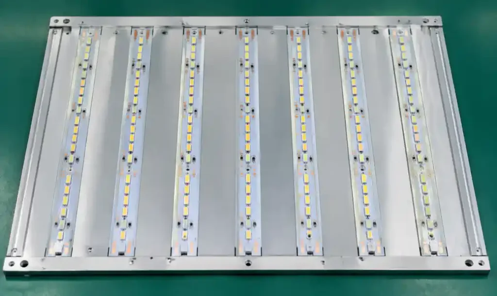
LED strip panels use linear arrangements optimized for utilization and efficiency. Single-row panels arrange 10-20 strips side-by-side with 5-8mm spacing, achieving 75-85% utilization on 300×400mm panels. This allows V-scoring between strips while maintaining rigidity.
Double-row arrays stack strips in parallel rows with center rails, reaching 85-92% utilization. Center support provides stability during reflow and test access. Material waste drops from 15-20% to 8-12% versus single-row layouts.
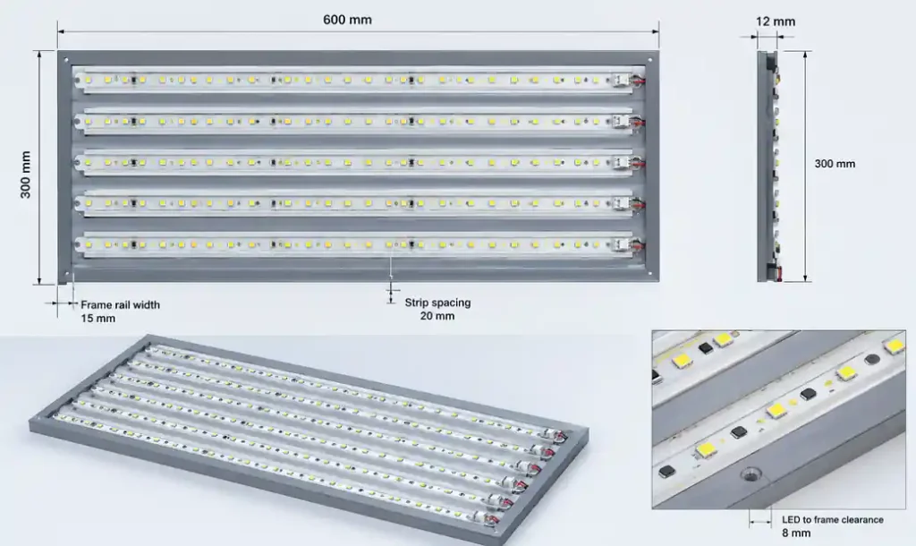
Step-and-repeat patterns arrange shorter strips (50-150mm) in grids for multiple lengths. This requires tab routing due to non-linear paths. Grid patterns maximize density but increase depaneling time by 40-60%.
| Panel Layout | Strips per Panel | Material Utilization | Depaneling Method | Cycle Time |
|---|---|---|---|---|
| Single-row linear | 10-15 strips | 75-85% | V-scoring | Baseline |
| Double-row linear | 20-30 strips | 85-92% | V-scoring | +15% |
| Step-and-repeat grid | 25-40 strips | 88-94% | Tab routing | +40-60% |
V-Groove Scoring Limitations on Aluminum Substrates
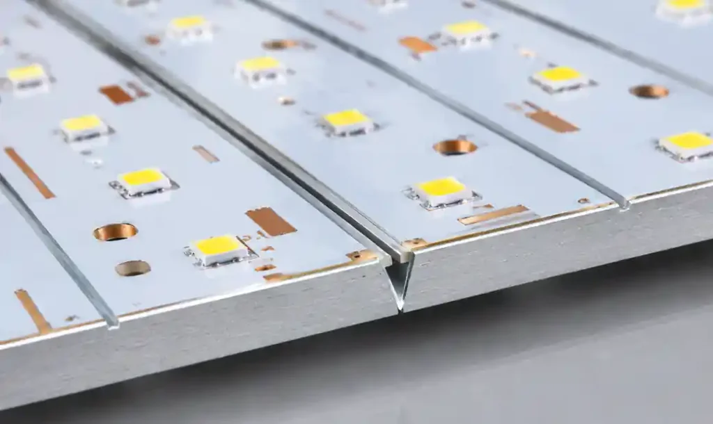
V-scoring aluminum MCPCB differs from FR4 due to material ductility and thermal expansion. Aluminum exhibits 23×10⁻⁶/°C coefficient of thermal expansion versus FR4’s 14-17×10⁻⁶/°C, creating residual stress along score lines during temperature cycling.
Standard V-scoring cuts 30-45° grooves leaving 0.3-0.4mm remaining thickness. Aluminum’s ductility causes tool wear 3-5× faster than FR4, requiring PCD (polycrystalline diamond) or carbide cutters replaced every 500-800 linear meters. Worn tools create rough surfaces that increase separation force by 40-70%.
Scoring depth control is critical. Grooves exceeding 70% thickness bow during reflow when gradients reach 2-4°C/mm across panel width. Shallow scores below 50% require excessive force that stresses solder joints. Optimal depth for 1.6mm aluminum MCPCB maintains 0.5-0.6mm remaining thickness.
V-scoring only works for straight separation lines. Curved ends or irregular outlines require tab routing. Aluminum panels with dielectric exceeding 150μm show delamination risk when separation force exceeds 8-10 N/mm.
Routing with Tabs for Aluminum Metal Core PCB
Tab routing mills through full aluminum substrate, leaving tabs securing strips to frame. Each strip uses 3-6 tabs with 2-4mm width × 5-8mm length providing holding strength without excessive break force.
Aluminum routing requires 2-3mm carbide end mills at 24,000-36,000 RPM with 1.5-2.5 m/min feeds. Slower feeds or dull tools generate heat softening dielectric, causing copper delamination within 3-5mm of edges.
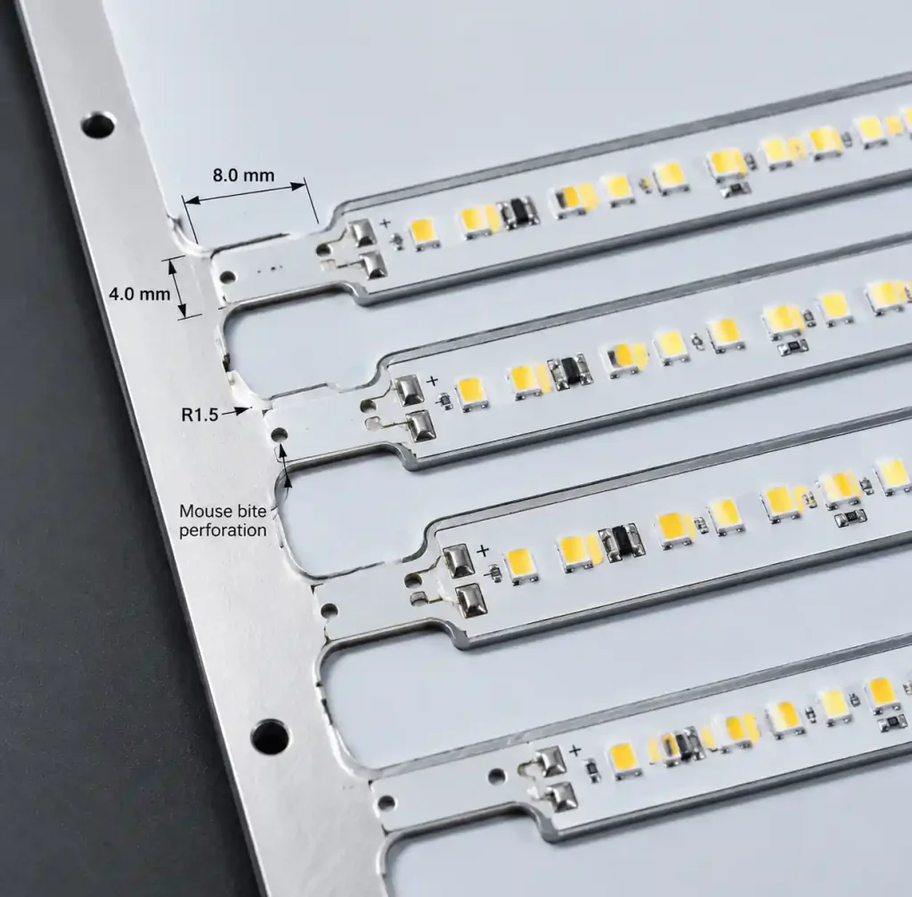
Position tabs minimum 15mm from LEDs to prevent stress transfer. Distribute evenly with maximum 80-100mm spacing to prevent warping during 260°C reflow. Use radiused connections with 0.5-1.0mm fillet radius versus sharp corners. Mouse bite perforations with 0.5mm holes spaced 0.5-1.0mm apart reduce separation force by 60-75%.
| Tab Parameter | Aluminum MCPCB | Standard FR4 | Critical Factor |
|---|---|---|---|
| Tab width | 2-4mm | 1.5-3mm | Aluminum ductility |
| Tab spacing | 80-100mm | 100-150mm | Reflow warping |
| Router speed | 24,000-36,000 RPM | 18,000-24,000 RPM | Heat generation |
| Break force | 15-25 N per tab | 8-15 N per tab | Material strength |
Thermal Management Across Panel Arrays
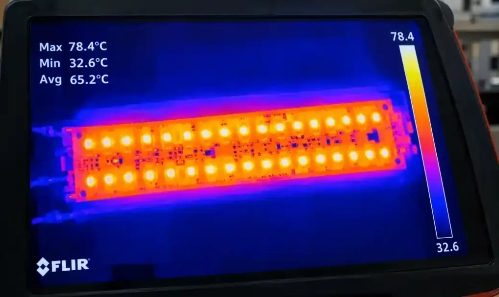
Aluminum provides superior thermal spreading versus FR4, but panel design determines junction temperature uniformity. A 300×400mm panel with 20 strips experiences 15-25°C gradients if thermal mass is unbalanced, stressing solder joints.
Frame width of 10-15mm provides mechanical support while minimizing thermal lag. Wider frames (20-30mm) create thermal reservoirs lagging strip areas by 8-12°C during peak reflow, causing incomplete solder wetting. Narrower frames below 8mm risk warping at 260°C.
Maintain consistent copper coverage (30-60%) across strips for uniform heating. Significant copper imbalances create differential heating causing bowing and placement errors during SMT.
Standard 3.2mm tooling holes positioned 5mm from edges enable heat sink mounting during testing. Verify temperature uniformity within ±5°C across all LED positions using thermal imaging at 260°C reflow simulation.
Electrical Testing Considerations for LED Strip Panels
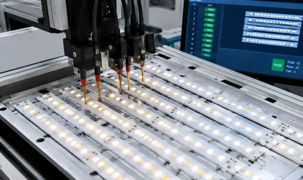
LED strip panels require electrical testing before depaneling while boards remain mechanically supported. Flying probe testers access test points through panel frame openings, verifying LED polarity, driver functionality, and open/short conditions without custom fixtures.
Position test points along strip edges within 3mm of panel frame for probe access. Maintain 2.5mm spacing between adjacent points for 0.7mm probe clearance. Use 1.0mm diameter pads with ENIG surface finish withstanding 10,000+ probe contacts.
Functional testing requires current injection through driver circuits while measuring forward voltage and luminous output. Design test points accessing LED anode/cathode connections and driver signals. Integrated testing validates protection circuits, current regulation, and thermal shutdown before final assembly.
Panel-level continuity testing verifies aluminum substrate grounding and thermal path integrity per IPC-6012 Class 2 requirements. Test between frame ground points and LED cathodes confirming >100MΩ isolation at 500V for safety-rated lighting products.
Depaneling Without Damage to Aluminum MCPCB
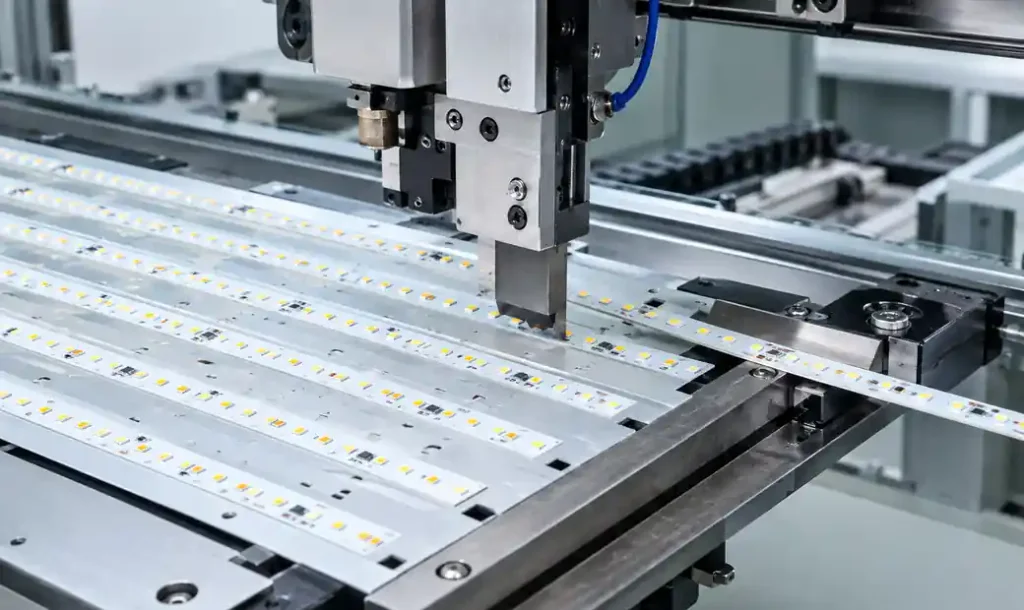
Manual depaneling of V-scored aluminum panels uses controlled bending with support fixtures limiting flexion to 2-3mm displacement. Excessive bending beyond 15-20° creates plastic deformation propagating microcracks into circuits. Support fixtures should contact surfaces within 10mm of score lines.
Automated equipment applies precise separation force through linear actuators. Set force limits to 150-200% of calculated score strength to accommodate aluminum work hardening without over-stressing joints. Force monitoring should reject panels requiring >120% nominal force, indicating dull tools or improper depth.
Router-based depaneling mills remaining tabs using 1.5-2.0mm end mills at reduced feeds (1.0-1.5 m/min) preventing burr formation. Climb milling produces cleaner edges than conventional milling, reducing burrs from 0.15mm to <0.05mm. Vacuum systems must capture conductive aluminum chips.
Laser depaneling offers non-contact separation for sensitive components. UV or green lasers ablate 0.3-0.5mm aluminum along separation paths without mechanical stress. Processing requires 15-25 seconds per linear meter versus 3-5 seconds for mechanical methods, cost-effective only when stress cannot be tolerated.
Design Rules for MCPCB LED Strip Panelization
Keep components minimum 5mm from panel edges and 3mm from score lines. This prevents damage during depaneling and allows probe access. LEDs closer than 3mm experience 40-60% higher stress that can crack ceramic substrates.
Specify 5-8mm spacing between strips for V-scoring clearance and thermal management. Spacing below 4mm weakens panel integrity. Wider spacing above 10mm reduces utilization below 80%.
Maintain balanced copper coverage across panel preventing differential expansion. Vary copper density by less than 20% between strips. Large imbalances cause warping leading to placement errors.
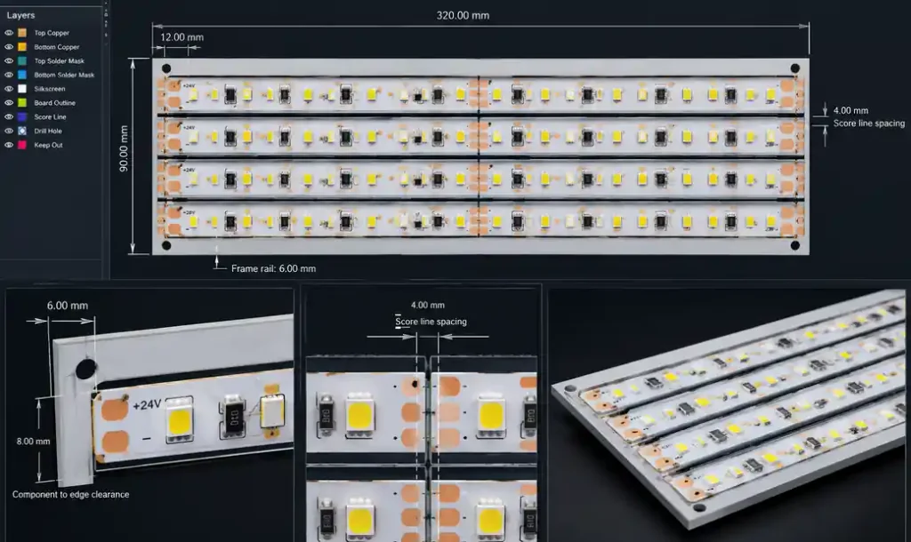
Frame rail width of 10-15mm balances support and material utilization. Include four tooling holes per panel sized 3.2mm for SMT registration. Aluminum base should extend uniformly without pockets creating thermal discontinuities.
| Design Parameter | Recommended Value | Critical For |
|---|---|---|
| Component to edge clearance | ≥5mm | Depaneling safety |
| Component to score line | ≥3mm | Stress prevention |
| Strip spacing (V-score) | 5-8mm | Tool clearance |
| Frame rail width | 10-15mm | Support vs. waste |
| Copper coverage variance | <20% between strips | Thermal uniformity |
| Tooling hole diameter | 3.2mm | SMT registration |
FAQ
Can you use standard PCB panelization methods for aluminum MCPCB?
No, aluminum requires modified approaches because higher ductility and thermal expansion create different behavior than FR4. V-scoring tools wear 3-5× faster requiring PCD or carbide cutters. Score depth control is more critical—aluminum needs 0.5-0.6mm remaining thickness versus 0.3-0.4mm for FR4. Separation force increases 50-80% due to aluminum’s mechanical strength.
What is the best depaneling method for LED strip MCPCB?
V-scoring offers fastest depaneling for straight strips, processing 5-10 panels per minute. Tab routing with mouse bites provides better edge quality and supports irregular shapes but increases time by 40-60%. Laser depaneling eliminates mechanical stress for sensitive packages but costs 4-6× more per panel. Choose based on geometry, volume, and component sensitivity.
How does aluminum panelization affect LED thermal performance?
Panel-level design determines junction temperature uniformity. Balanced copper coverage maintains ±5°C uniformity during reflow preventing expansion stress. Frame width 10-15mm minimizes thermal lag while providing support. Continuous aluminum coverage ensures heat spreading—localized cutouts create hot spots reducing LED lifespan by 30-50%.
What spacing do you need between LED strips in a panel?
Linear panels require 5-8mm spacing for V-scoring tool clearance and thermal management. Spacing below 4mm weakens integrity during 260°C reflow. Spacing above 10mm reduces utilization below 80% without benefits. The 5-8mm range achieves 85-92% utilization while maintaining rigidity and testing access.
Why do aluminum panels require different V-scoring depth than FR4?
Aluminum’s thermal expansion (23×10⁻⁶/°C) exceeds FR4 (14-17×10⁻⁶/°C), creating higher stress during temperature cycling. Scoring too deep (>70%) causes bowing during reflow when gradients reach 2-4°C/mm. Optimal depth for 1.6mm aluminum maintains 0.5-0.6mm remaining thickness, balancing separation force against thermal stress resistance.
How do you prevent solder joint damage during depaneling?
Maintain 3mm clearance between LEDs and score lines reducing stress transfer by 40-60%. Use support fixtures contacting boards within 10mm of separation points, limiting flexion to 2-3mm and angles below 15-20°. Set automated force limits to 150-200% of calculated score strength. For ceramic packages, specify laser depaneling eliminating mechanical stress.
Conclusion
MCPCB panelization for LED strip manufacturing requires specialized strategies accounting for aluminum substrate properties different from FR4. Linear panel layouts achieve 85-92% material utilization with proper strip spacing and frame geometry. V-scoring provides cost-effective depaneling for straight strips when scoring depth maintains 0.5-0.6mm remaining thickness, while tab routing supports irregular shapes.
Thermal management across panels ensures ±5°C temperature uniformity through balanced copper coverage and optimized frame width. Electrical testing before depaneling identifies defects while boards remain supported. Proper depaneling methods prevent solder joint damage through controlled force application and component clearance design.
If you need MCPCB manufacturing for LED strips, Andwin Circuits offers metal core PCB capabilities up to 3mm aluminum thickness with thermal conductivity from 1.0 to 8.0 W/m·K. We provide optimized panelization design, automated testing, and precision depaneling protecting LED assemblies. ISO 9001 and UL certified with fast delivery in 7-15 days. Contact us today for panelization design review and turnkey manufacturing solutions.