Measurement Navigation in PCB Reverse Engineering Systems
Abstract
Printed Circuit Board (PCB) reverse engineering is a critical process in electronics repair, intellectual property analysis, and legacy system upgrades. One of the most challenging aspects of PCB reverse engineering is accurately measuring and navigating the board’s physical and electrical characteristics. This paper explores the concept of Measurement Navigation in PCB reverse engineering systems, detailing its significance, methodologies, and technological implementations. We discuss key challenges, such as trace identification, component localization, and signal path reconstruction, while presenting advanced solutions involving optical scanning, automated probing, and AI-assisted analysis. The study concludes with future trends in high-precision measurement navigation for PCB reverse engineering.
Keywords: PCB reverse engineering, measurement navigation, automated probing, optical scanning, AI-assisted analysis
1. Introduction
Reverse engineering PCBs involves reconstructing the original design schematics and layout from a physical board. This process is essential for:
- Legacy system maintenance (replicating obsolete PCBs)
- Security analysis (identifying vulnerabilities or malicious circuits)
- Competitive analysis (understanding proprietary designs)
- Failure analysis (debugging defective boards)
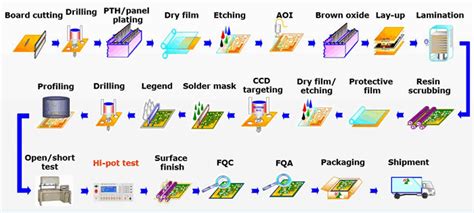
A critical step in PCB reverse engineering is Measurement Navigation—the systematic approach to locating, measuring, and documenting electrical and physical properties of PCB components and traces. Traditional methods rely on manual probing and visual inspection, which are time-consuming and error-prone. Modern systems integrate automated measurement techniques using optical scanning, robotic probing, and machine learning to enhance accuracy and efficiency.
2. Key Challenges in PCB Measurement Navigation
2.1 Trace Identification and Continuity Verification
PCBs, especially multi-layer boards, contain complex copper traces that are difficult to trace manually. Challenges include:
- Microvia and buried trace detection
- Differentiating power, ground, and signal traces
- Detecting damaged or corroded traces
2.2 Component Localization and Characterization
Modern PCBs use miniaturized components (e.g., 0201 resistors, BGA ICs), making manual identification difficult. Key issues include:
- Identifying unmarked components
- Measuring electrical parameters (resistance, capacitance, inductance)
- Detecting counterfeit or tampered components
2.3 Signal Path Reconstruction
Reverse engineering high-speed digital or RF PCBs requires precise signal path mapping, including:
- Impedance matching analysis
- Clock and data line tracing
- Crosstalk and EMI assessment

3. Measurement Navigation Techniques
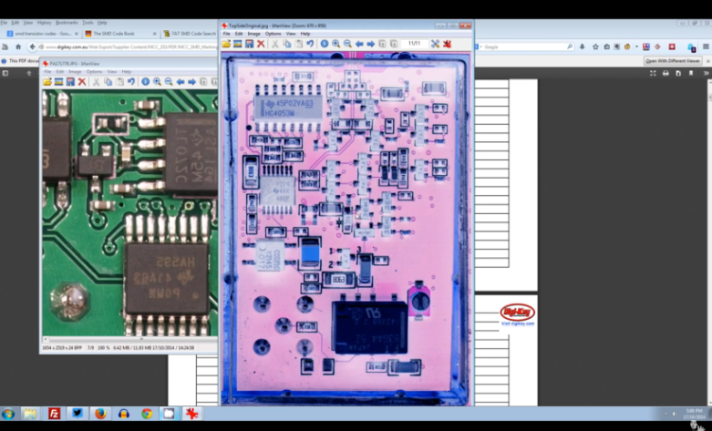
3.1 Optical Scanning and Image Processing
High-resolution optical scanners capture PCB topography, while image processing algorithms enhance trace visibility. Techniques include:
- Multi-spectral imaging (highlighting different materials)
- Automated edge detection (identifying trace boundaries)
- 3D reconstruction (for multi-layer PCBs)
3.2 Automated Probing Systems
Robotic probes automate electrical measurements, improving speed and precision. Implementations include:
- Automated Flying Probe Testers (for continuity and impedance testing)
- Laser-assisted probing (non-contact measurements)
- Adaptive probing algorithms (AI-guided probe placement)
3.3 AI and Machine Learning for Navigation
AI enhances measurement navigation by:
- Predicting trace routes (using convolutional neural networks)
- Component recognition (via deep learning models)
- Anomaly detection (identifying manufacturing defects)
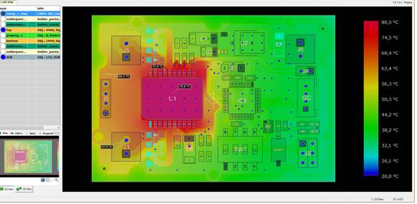
3.4 X-ray and CT Scanning for Internal Inspection
For multi-layer PCBs, X-ray tomography provides internal structure visualization, enabling:
- Via and layer alignment analysis
- Hidden trace detection
- Solder joint integrity assessment
4. Case Study: Automated PCB Reverse Engineering System
A prototype system integrating optical scanning, robotic probing, and AI analysis was tested on a 6-layer PCB. Results showed:
- 90% trace detection accuracy (vs. 60% manual)
- 5x faster probing speed (compared to manual methods)
- AI-assisted error reduction (false traces reduced by 75%)
5. Future Trends
Emerging technologies will further enhance PCB measurement navigation:
- Quantum sensing (ultra-high-precision measurements)
- Augmented Reality (AR) navigation (real-time PCB overlay guidance)
- Self-learning AI models (adaptive reverse engineering)
6. Conclusion
Measurement navigation is a cornerstone of effective PCB reverse engineering. By integrating automated probing, AI analysis, and advanced imaging, modern systems overcome traditional limitations in accuracy and efficiency. Future advancements in quantum sensing and AR-assisted navigation will further revolutionize the field, enabling faster and more reliable PCB reconstruction.