Measurement of PCB Trace Width: Techniques and Best Practices
Abstract
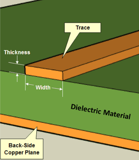
Printed Circuit Board (PCB) trace width is a critical parameter that affects the electrical performance, thermal management, and reliability of electronic circuits. Accurate measurement of trace width ensures compliance with design specifications and manufacturing tolerances. This paper explores various techniques for measuring PCB trace width, including optical microscopy, profilometry, cross-sectional analysis, and automated optical inspection (AOI). Additionally, factors influencing trace width accuracy, such as etching processes and material properties, are discussed. Best practices for trace width measurement and verification are also presented to enhance PCB manufacturing quality.
1. Introduction
PCBs serve as the backbone of modern electronics, providing electrical connections between components through conductive traces. The width of these traces is crucial because it determines current-carrying capacity, impedance, and heat dissipation. Deviations from the designed trace width can lead to signal integrity issues, excessive heating, or even circuit failure. Therefore, precise measurement of PCB trace width is essential in both prototyping and mass production.
This paper reviews different measurement techniques, their advantages and limitations, and industry best practices to ensure accurate and repeatable results.
2. Importance of PCB Trace Width
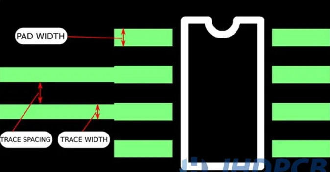
Trace width impacts several key aspects of PCB performance:
- Current Carrying Capacity: Wider traces can handle higher currents without excessive heating (as described by IPC-2152 standards).
- Impedance Control: High-frequency signals require controlled trace widths to maintain characteristic impedance (e.g., 50Ω for RF circuits).
- Manufacturing Tolerances: Variations in etching and plating processes can alter trace width, affecting signal integrity.
- Thermal Management: Narrow traces may overheat, leading to premature failure.
Thus, verifying trace width ensures that the PCB meets design requirements and functional expectations.
3. Techniques for Measuring PCB Trace Width
3.1 Optical Microscopy
Optical microscopy is one of the most common methods for measuring trace width. A high-magnification microscope with a calibrated reticle or digital imaging software is used to examine the traces.
Advantages:
- Non-destructive and quick.
- Suitable for both lab and production environments.
- High-resolution imaging allows for precise edge detection.
Limitations:
- Limited depth perception may affect measurements on uneven surfaces.
- Requires proper lighting and focus to avoid parallax errors.
3.2 Laser Scanning Confocal Microscopy
This advanced technique uses a laser beam to scan the PCB surface, generating a 3D profile of the trace. It provides high-resolution measurements of width and height.
Advantages:
- High accuracy (±0.1 µm).
- Measures both width and thickness simultaneously.
- Non-contact method reduces risk of damage.
Limitations:
- Expensive equipment.
- Slower than optical microscopy.
3.3 Contact Profilometry
A stylus profilometer physically traces the PCB surface, recording variations in height and width.
Advantages:
- Direct measurement with high precision.
- Works on reflective and non-reflective surfaces.
Limitations:
- Risk of damaging fine traces due to mechanical contact.
- Slower than optical methods.
3.4 Cross-Sectional Analysis
In this destructive method, the PCB is cut perpendicular to the trace, and the cross-section is polished and examined under a microscope.
Advantages:
- Provides exact width and thickness measurements.
- Reveals internal structure (e.g., plating uniformity).
Limitations:
- Destructive—sample is lost after measurement.
- Time-consuming sample preparation.
3.5 Automated Optical Inspection (AOI)
AOI systems use high-resolution cameras and image processing algorithms to measure trace width across entire PCBs.
Advantages:
- Fast and scalable for mass production.
- Detects defects (e.g., under-etching, over-etching).
Limitations:
- Requires calibration and programming.
- May miss subtle variations without high-end optics.
4. Factors Affecting Trace Width Accuracy
4.1 Etching Process Variations
Chemical etching can cause undercutting or over-etching, leading to deviations from the designed trace width.
4.2 Copper Foil Thickness
Variations in copper thickness (e.g., 1 oz vs. 2 oz) affect the final trace width after etching.
4.3 Photolithography Resolution
The quality of the photomask and exposure process influences trace definition.
4.4 Plating and Surface Finish
Electroplating (e.g., ENIG, HASL) can add thickness, slightly altering trace dimensions.
5. Best Practices for Trace Width Measurement
- Calibration: Regularly calibrate measurement tools using certified standards.
- Multiple Sampling: Measure traces at different locations to account for process variations.
- Edge Detection Algorithms: Use software-based edge detection for consistent optical measurements.
- Cross-Validation: Combine multiple methods (e.g., microscopy + profilometry) for critical traces.
- Environmental Control: Ensure stable temperature and humidity to prevent material expansion/contraction.
6. Conclusion
Accurate PCB trace width measurement is vital for ensuring circuit performance and reliability. Various techniques—from optical microscopy to AOI—offer different trade-offs in speed, accuracy, and cost. Manufacturers must select the appropriate method based on application requirements and implement best practices to minimize measurement errors. As PCB technology advances toward finer pitches and higher frequencies, trace width measurement will remain a key quality control step in electronics manufacturing.