Methods for Identifying PCB Faults: A Comprehensive Guide
Printed Circuit Boards (PCBs) are the backbone of modern electronics, found in everything from consumer gadgets to industrial machinery. However, like any electronic component, PCBs are prone to faults due to manufacturing defects, environmental factors, or wear and tear. Identifying and diagnosing PCB faults efficiently is crucial for minimizing downtime and repair costs. This article explores various methods for detecting PCB faults, ranging from visual inspection to advanced diagnostic techniques.
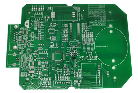
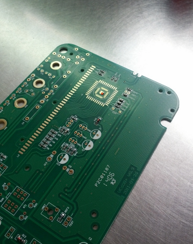
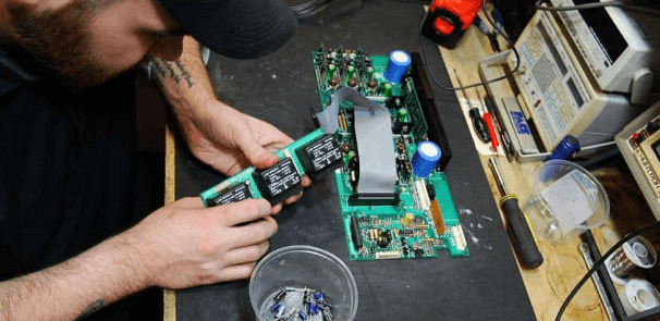
1. Visual Inspection
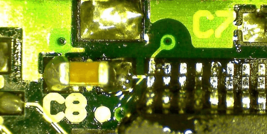
The first and simplest method for identifying PCB faults is a thorough visual inspection. Many defects can be spotted with the naked eye or using a magnifying glass/microscope.
Common Visual Defects:
- Solder Bridges: Unintended connections between adjacent solder joints.
- Cracked Traces: Physical damage to conductive pathways.
- Burnt Components: Discoloration or charring due to overheating.
- Lifted Pads: Detached copper pads from the PCB surface.
- Cold Solder Joints: Dull, grainy, or improperly formed solder connections.
- Component Misalignment: Incorrectly placed or misoriented parts.
Tools for Visual Inspection:
- Magnifying Glass/Loupe (for basic checks)
- Microscope (for fine-pitch components)
- Digital Camera with Macro Lens (for documentation)
- UV Light (to detect flux residues or contamination)
2. Multimeter Testing
A digital multimeter (DMM) is essential for checking electrical continuity, resistance, and voltage levels.
Key Multimeter Tests:
- Continuity Test: Ensures no open circuits in traces.
- Resistance Measurement: Detects short circuits or abnormal resistance in components.
- Voltage Testing: Verifies power supply levels at different PCB points.
- Diode & Transistor Checks: Confirms semiconductor functionality.
Limitations:
- Cannot detect intermittent faults.
- Time-consuming for complex PCBs.
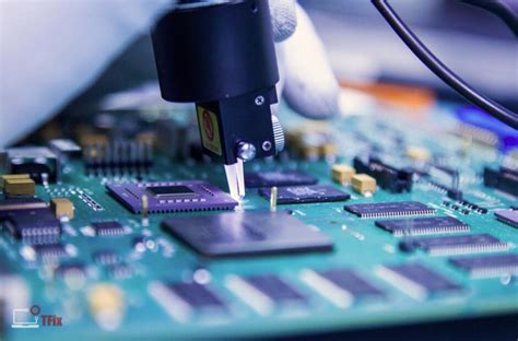
3. Oscilloscope Analysis
An oscilloscope helps analyze signal integrity and timing issues.
Applications:
- Signal Tracing: Verifies waveform shapes (e.g., square, sine, or distorted signals).
- Noise Detection: Identifies unwanted oscillations or interference.
- Timing Verification: Ensures clock signals and data lines operate correctly.
Advanced Techniques:
- Differential Probing: For high-speed signals.
- FFT Analysis: Detects frequency-related anomalies.
4. Thermal Imaging (Infrared Cameras)
Overheating components often indicate faults such as short circuits or failing ICs.
How It Works:
- Infrared cameras detect heat patterns.
- Hotspots reveal excessive current draw or poor thermal management.
Common Findings:
- Overheated ICs (due to internal shorts or excessive load).
- Cold Solder Joints (poor thermal conduction).
- Failing Power Components (MOSFETs, regulators).
5. Automated Optical Inspection (AOI)
AOI systems use high-resolution cameras and AI algorithms to scan PCBs for defects.
Advantages:
- High-Speed Detection: Faster than manual inspection.
- Precision: Identifies microscopic defects.
- Consistency: Reduces human error.
Commonly Detected Issues:
- Solder Defects (insufficient/excess solder).
- Missing Components.
- Misaligned Parts.
6. X-Ray Inspection (AXI)
For multilayer PCBs and BGAs (Ball Grid Arrays), X-ray inspection is indispensable.
Applications:
- Internal Trace Damage: Detects breaks in hidden layers.
- Solder Voids: Finds insufficient solder in BGA joints.
- Component Integrity: Checks internal wire bonds.
Limitations:
- Expensive equipment.
- Requires trained operators.
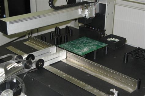
7. In-Circuit Testing (ICT)
ICT uses bed-of-nails fixtures to test individual components while powered.
Key Features:
- Measures Resistance, Capacitance, Inductance.
- Detects Open/Short Circuits.
- Verifies Component Values (resistors, capacitors, etc.).
Limitations:
- Requires custom test fixtures.
- Less effective for high-frequency signals.
8. Functional Testing (FCT)
FCT evaluates the PCB’s real-world performance by simulating operational conditions.
Methods:
- Firmware Validation: Ensures microcontrollers execute code correctly.
- Input/Output Testing: Checks sensors, displays, and communication interfaces.
- Load Testing: Verifies stability under maximum current draw.
Advantages:
- Confirms overall functionality.
- Detects intermittent issues missed by other tests.
9. Boundary Scan Testing (JTAG)
JTAG (IEEE 1149.1) is used for testing digital ICs without physical probes.
How It Works:
- Scan Chains: Test interconnections between ICs.
- Fault Isolation: Pinpoints defective components.
Best For:
- High-Density PCBs.
- BGAs and Complex ICs.
10. Signal Integrity Analysis
For high-speed PCBs, signal integrity issues (reflections, crosstalk) can cause failures.
Tools Used:
- Vector Network Analyzer (VNA).
- Time-Domain Reflectometer (TDR).
Common Fixes:
- Impedance Matching.
- Redesigning Trace Layouts.
Conclusion
Finding PCB faults requires a systematic approach, combining visual checks, electrical testing, and advanced diagnostics. The best method depends on the PCB’s complexity and the type of fault suspected. For hobbyists, a multimeter and oscilloscope may suffice, while manufacturers rely on AOI, X-ray, and JTAG for precision. By leveraging these techniques, engineers and technicians can efficiently diagnose and repair PCB faults, ensuring reliable electronic performance.