Methods to Distinguish the Number of Layers in PCB Motherboards and Graphics Cards
Introduction
Printed Circuit Boards (PCBs) are essential components in modern electronics, serving as the foundation for motherboards and graphics cards. One critical aspect of PCB design is the number of layers, which directly impacts performance, signal integrity, and power delivery. Determining whether a PCB is a 4-layer, 6-layer, 8-layer, or even higher-layer design can be challenging without proper techniques. This article explores various methods to distinguish the number of layers in PCBs, specifically focusing on motherboards and graphics cards.
1. Visual Inspection Methods
1.1 Observing PCB Edge Layers
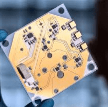
The simplest way to estimate the number of layers in a PCB is by examining its cross-section. If the board is not coated with solder mask or conformal coating, the layers may be visible at the edges. Each conductive layer is separated by an insulating dielectric material (usually FR-4). By counting the alternating copper and dielectric layers, one can estimate the total number of layers.
- 4-layer PCB: Typically shows two inner layers sandwiched between top and bottom layers.
- 6-layer PCB: Displays additional internal signal or power planes.
- 8-layer and above: More complex, with multiple internal layers for high-speed signals and power distribution.
However, many modern PCBs have black or green solder masks that obscure the internal layers, making this method less reliable.
1.2 Via Inspection
Vias (plated through-holes) are used to connect different PCB layers. By examining via structures, we can infer layer count:
- Through-hole vias: Span the entire board, indicating multiple layers.
- Blind vias: Connect an outer layer to an inner layer without going through the entire board (common in high-layer-count PCBs).
- Buried vias: Connect only internal layers, invisible from the outside (used in advanced designs like 8+ layer PCBs).
If a PCB has blind or buried vias, it likely has a higher layer count (6+ layers).
2. Technical Documentation and Manufacturer Specifications
2.1 Checking PCB Markings
Some PCBs have markings indicating layer count, such as:
- “4L” for 4-layer
- “6L” for 6-layer
- “8L” for 8-layer
These markings are often found near the PCB model number or manufacturer logo.
2.2 Reviewing Datasheets and Schematics
Motherboard and GPU manufacturers sometimes disclose PCB layer counts in technical documentation. For example:
- Entry-level motherboards: Typically 4-6 layers.
- High-end motherboards and GPUs: Often 8-12 layers or more for better power delivery and signal integrity.
If official documentation is unavailable, community forums (such as Overclock.net or TechPowerUp) may provide insights from user teardowns.
3. X-ray and Microsectioning Analysis
3.1 X-ray Imaging
X-ray inspection allows non-destructive examination of internal PCB layers. This method is commonly used in industrial quality control and reverse engineering.
- Advantages: Non-invasive, reveals hidden vias and layer stack-up.
- Disadvantages: Requires specialized equipment, not practical for consumers.
3.2 Microsectioning (Destructive Testing)
For precise analysis, a small section of the PCB can be cut and polished to expose the internal layers under a microscope.
- Process:
- Cut a small PCB sample.
- Polish the cross-section.
- Examine under magnification to count layers.
- Limitations: Destructive, not suitable for functional boards.

4. Signal and Power Plane Analysis
4.1 Power Delivery Network (PDN) Complexity
High-layer-count PCBs (e.g., 8+ layers) often have dedicated power and ground planes to reduce noise and improve stability.
- Motherboards:
- Budget models: 4-6 layers (shared power planes).
- Premium models: 8+ layers (separate planes for CPU, RAM, PCIe).
- Graphics Cards:
- Mid-range GPUs: 6-8 layers.
- High-end GPUs (e.g., NVIDIA RTX 4090, AMD RX 7900 XTX): 10-12+ layers for better power delivery and signal integrity.
4.2 High-Speed Signal Routing
More layers allow better isolation of high-speed signals (PCIe, DDR, USB). If a PCB has multiple impedance-controlled traces, it likely has a higher layer count.
5. Comparative Analysis with Known PCBs
5.1 Comparing PCB Thickness
While not always accurate, thicker PCBs tend to have more layers:
- 4-layer: ~1.2mm – 1.6mm
- 6-layer: ~1.6mm – 2.0mm
- 8-layer+: >2.0mm
However, advanced manufacturing can produce thin, high-layer-count PCBs, so this is not a definitive method.
5.2 Benchmarking Against Known Designs
By comparing a PCB with known reference designs (e.g., NVIDIA Founders Edition vs. third-party GPUs), one can estimate layer counts based on similar layouts.
Conclusion
Determining the number of layers in a PCB motherboard or graphics card requires a combination of visual inspection, via analysis, technical documentation, and sometimes advanced techniques like X-ray imaging. While some methods are accessible to hobbyists (e.g., edge inspection, via counting), others require professional tools. Understanding PCB layer counts helps in assessing board quality, performance potential, and manufacturing complexity.
For consumers, checking manufacturer specifications and community teardowns remains the most practical approach, while engineers and analysts may resort to microsectioning or X-ray inspection for precise verification.