Methods to Improve Defect Rates in Automotive PCBs
Introduction
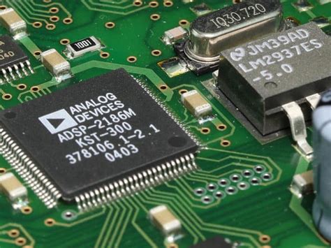
Printed Circuit Boards (PCBs) are critical components in modern automotive electronics, supporting functions such as engine control, infotainment systems, advanced driver-assistance systems (ADAS), and electric vehicle (EV) power management. As vehicles become more reliant on electronic systems, the demand for high-reliability PCBs has increased. However, defects in automotive PCBs can lead to failures that compromise safety, performance, and durability.
Reducing PCB defect rates requires a systematic approach, encompassing design optimization, material selection, manufacturing process control, and rigorous testing. This article explores key methods to improve automotive PCB defect rates, ensuring higher reliability and compliance with industry standards such as IPC-A-600 and IATF 16949.
1. Design Optimization for Manufacturability (DFM)
1.1 Proper Layout and Routing
- Minimize Signal Integrity Issues: High-speed signals in automotive applications (e.g., CAN bus, Ethernet) require controlled impedance routing to prevent signal degradation.
- Avoid High-Density Traces: Excessive trace crowding increases the risk of short circuits and crosstalk.
- Thermal Management: Proper heat dissipation through thermal vias and copper pours prevents overheating-related failures.
1.2 Component Placement and Footprint Design
- Avoid Tombstoning: Uneven heating during reflow soldering can cause small passive components (e.g., resistors, capacitors) to lift on one end. Symmetric pad design helps mitigate this.
- Adequate Spacing: Components should be spaced to prevent solder bridging and facilitate automated assembly.
1.3 Design Rule Checks (DRC) and Simulation
- Use automated DRC tools to identify potential manufacturing issues before production.
- Perform signal integrity and thermal simulations to optimize performance.
2. Material Selection for Automotive-Grade PCBs
2.1 High-Temperature Substrates
- Automotive PCBs must withstand extreme temperatures (e.g., -40°C to 150°C). Materials like FR-4 HTG (High-Tg), polyimide, and ceramic-filled laminates offer better thermal stability.
2.2 Copper Quality and Thickness
- Use high-purity copper to reduce resistive losses and improve current-carrying capacity.
- Heavy copper PCBs (2 oz and above) are preferred for power electronics in EVs.
2.3 Conformal Coatings
- Coatings such as acrylic, silicone, or polyurethane protect PCBs from moisture, dust, and chemical exposure.
3. Advanced Manufacturing Process Control
3.1 Automated Optical Inspection (AOI)
- AOI systems detect defects like missing components, misalignment, solder bridges, and insufficient solder before reflow.
3.2 Solder Paste Application and Reflow Profiling
- Stencil Design: Optimal aperture size ensures correct solder paste deposition.
- Reflow Profile Optimization: Temperature ramps must be carefully controlled to prevent voids, cold joints, or component damage.
3.3 Via Filling and Plating Quality
- Filled and capped vias improve reliability in high-vibration environments.
- Electroless Nickel Immersion Gold (ENIG) or Immersion Silver (IAg) finishes enhance solderability and corrosion resistance.
3.4 Cleanliness and Contamination Control
- Ionic contamination can cause electrochemical migration (dendrite growth). Post-assembly cleaning (e.g., ultrasonic or plasma cleaning) is essential.
4. Rigorous Testing and Quality Assurance
4.1 In-Circuit Testing (ICT) and Flying Probe Testing
- ICT checks for open circuits, shorts, and component values.
- Flying probe testing is flexible for low-to-medium volume production.
4.2 Environmental Stress Testing
- Thermal Cycling: Exposes PCBs to extreme temperature fluctuations to identify weak solder joints.
- Vibration and Shock Testing: Ensures reliability in harsh automotive conditions.
- Humidity Testing (HAST/THA): Evaluates resistance to moisture-induced failures.
4.3 Automated X-Ray Inspection (AXI)
- Detects hidden defects such as voids in BGA solder joints or internal layer misalignment.
4.4 Functional Testing
- Validates that the PCB performs as intended in real-world scenarios (e.g., power-up tests, communication bus validation).

5. Supplier and Supply Chain Management
5.1 Partnering with Certified PCB Manufacturers
- Suppliers should comply with IPC Class 3 (high-reliability) and IATF 16949 (automotive quality management) standards.
5.2 Incoming Material Inspection
- Verify raw materials (laminates, copper, solder paste) for compliance with specifications.
5.3 Traceability and Root Cause Analysis
- Implement barcode/RFID tracking to trace defects back to their source.
- Use Failure Mode and Effects Analysis (FMEA) to proactively address potential failure points.
6. Continuous Improvement and Data Analytics
6.1 Statistical Process Control (SPC)
- Monitor key process parameters (e.g., solder paste thickness, reflow temperatures) to detect deviations early.
6.2 Machine Learning for Defect Prediction
- AI-driven analytics can identify patterns in defect data, enabling predictive maintenance and process adjustments.
6.3 Feedback Loops with Design and Production Teams
- Regularly review defect trends and implement corrective actions.
Conclusion
Reducing defect rates in automotive PCBs requires a holistic approach, integrating design best practices, material selection, precision manufacturing, stringent testing, and supply chain control. By adopting advanced inspection technologies, optimizing processes, and leveraging data analytics, manufacturers can achieve higher yields and reliability, meeting the stringent demands of the automotive industry.
Investing in these methods not only minimizes costly rework and recalls but also enhances the safety and longevity of automotive electronic systems—a critical factor as vehicles evolve toward greater electrification and autonomy.