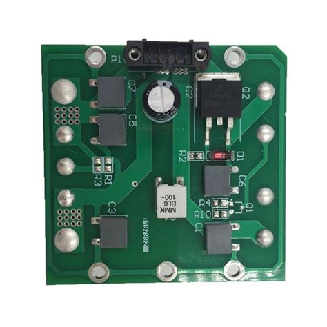
Microtek Inverter PCB Circuit Design and Optimization Strategies

Key Takeaways
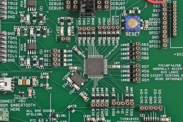
When designing PCB manufacturing solutions for Microtek inverters, you need to balance technical precision with cost-effective strategies. Start by prioritizing thermal management—ensuring proper heat dissipation through copper weight optimization and strategic component placement. For PCB manufacturing companies, selecting materials with high thermal conductivity (e.g., FR-4 with ceramic fillers) directly impacts reliability in industrial environments.
To minimize PCB manufacturing cost, adopt energy-efficient routing strategies, such as reducing trace lengths and avoiding right-angle bends, which lower resistive losses. Partnering with PCB manufacturing business specialists ensures access to advanced fabrication techniques like laser-drilled vias or embedded cooling channels.
| Design Factor | Optimization Strategy | Impact on Performance |
|---|---|---|
| Thermal Management | Multi-layer PCBs with thermal vias | Reduces hotspots by 20-30% |
| Component Selection | High-efficiency MOSFETs & capacitors | Improves power conversion by 15% |
| Routing Efficiency | Short, wide power traces | Lowers voltage drop by 10-12% |
When troubleshooting, always verify solder joint integrity and component alignment—common failure points in high-vibration settings. For deeper insights into industrial-grade standards, refer to this guide on PCB design compliance. By integrating these practices, you can achieve durable, high-performance inverter PCBs tailored for demanding applications.

Thermal Management in Microtek Inverter PCB Design
Effective thermal management forms the backbone of reliable high-power inverter PCB performance. When designing Microtek inverter PCBs, you must prioritize heat dissipation to prevent component degradation and ensure operational stability. Start by analyzing thermal hotspots through simulation tools, focusing on high-current components like IGBTs and diodes. Strategic placement of thermal vias and copper pours enhances heat transfer from critical areas to the board’s outer layers or heatsinks.
Collaborating with specialized PCB manufacturing companies ensures material choices align with thermal requirements—for instance, selecting high-Tg laminates or metal-core substrates for improved conductivity. However, balancing PCB manufacturing cost with performance is crucial; thicker copper traces (2–4 oz) reduce resistive losses but increase material expenses.
For industrial applications, integrate active cooling solutions such as thermally optimized heatsinks or fans, paired with thermal interface materials (TIMs) to minimize contact resistance. Layer stacking should separate heat-sensitive components from power stages, while conformal coatings protect against environmental factors.
Proactive thermal design not only extends PCB lifespan but also reduces long-term PCB manufacturing business risks linked to field failures. By embedding these practices early, you create a foundation for scalable, energy-efficient systems that meet stringent industrial demands.
Optimizing Power Conversion Efficiency in Microtek PCBs
Achieving peak power conversion efficiency in industrial-grade Microtek inverter PCBs requires balancing design precision with material science. Start by evaluating PCB manufacturing specifications—thicker copper layers (2–4 oz) reduce resistive losses, while low-loss dielectric substrates minimize signal degradation. When selecting PCB manufacturing companies, prioritize partners with expertise in high-current designs, as improper trace width calculations can increase heat generation by up to 20%.
Tip: Use thermal simulation tools during layout planning to identify hotspots before prototyping—this reduces PCB manufacturing cost by avoiding post-production revisions.
For high-frequency switching circuits, optimize the parasitic inductance of power traces by adopting a star-grounding topology. Pair this with low-ESR capacitors placed adjacent to MOSFETs or IGBTs to stabilize voltage ripple. If you’re managing a PCB manufacturing business, consider automated optical inspection (AOI) systems to ensure solder joint integrity, which directly impacts converter efficiency.
Layer stacking also plays a critical role: separate high-power and control signal layers with ground planes to mitigate electromagnetic interference (EMI). Partnering with PCB manufacturing specialists who offer advanced via-in-pad technology can further enhance thermal dissipation and electrical performance. Remember, even minor improvements in efficiency—like reducing conduction losses by 5%—compound significantly in 24/7 industrial operations.
Component Selection Strategies for Industrial Inverter PCBs
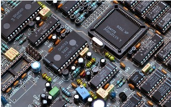
When selecting components for industrial-grade PCB manufacturing, prioritize voltage/current ratings and thermal resilience to match demanding operational conditions. Start by evaluating power semiconductors like IGBTs or MOSFETs—opt for devices with low switching losses and high current-carrying capacity to minimize heat generation. Collaborate with reputable PCB manufacturing companies to source components with proven reliability in high-vibration environments, as industrial applications often expose PCBs to mechanical stress.
Consider PCB manufacturing cost implications when choosing capacitors and inductors: high-quality film capacitors may have a higher upfront cost but offer longer lifespans, reducing maintenance expenses. For gate drivers, select isolated ICs that ensure noise immunity, critical for maintaining signal integrity in power-dense layouts. Always verify component footprints against your PCB manufacturing business’s assembly capabilities to avoid mismatches during production.
Integrate thermal derating curves and failure rate data into your selection process, particularly for passive components like resistors and fuses. This ensures compliance with industry standards while balancing performance and durability. By aligning component specifications with both electrical requirements and PCB manufacturing realities, you create designs that withstand industrial challenges without compromising efficiency or reliability.
Microtek PCB Layout Techniques for Enhanced Reliability
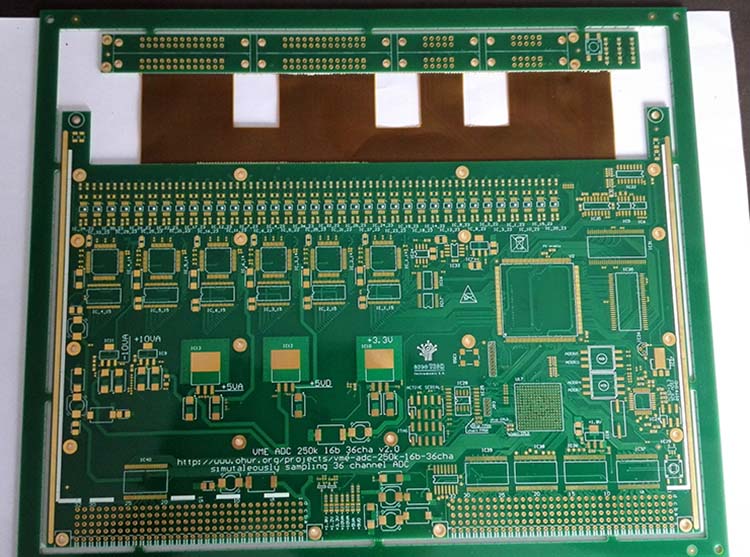
When designing inverter PCBs for industrial applications, prioritizing reliability begins with strategic trace routing and component placement. You’ll want to minimize electromagnetic interference (EMI) by separating high-power and low-voltage circuits, ensuring at least 4-6mm clearance between critical traces. Partnering with experienced PCB manufacturing companies ensures adherence to industrial-grade tolerances, particularly for multilayer boards requiring precise via placement and impedance control.
Thermal management directly impacts reliability, so integrate thermal relief pads and copper pours near heat-generating components like IGBTs. This reduces hot spots and extends component lifespan, especially when combined with PCB manufacturing processes that use high-temperature laminates. For cost-sensitive projects, balancing PCB manufacturing cost with material quality is critical—opting for FR-4 with a high Tg rating (≥170°C) strikes a practical balance.
Signal integrity hinges on ground plane optimization. A continuous ground layer beneath high-frequency circuits minimizes noise, while star grounding prevents ground loops. When prototyping, validate designs with PCB manufacturing business partners who offer rapid turnaround for iterative testing. Finally, ensure compliance with IPC-2221 standards for creepage and clearance, particularly in humid or dusty environments. These techniques not only enhance reliability but also align with broader goals of energy efficiency and fault tolerance discussed in subsequent sections.
Troubleshooting Common Microtek Inverter Circuit Issues
When diagnosing recurring problems in Microtek inverter circuits, start by isolating voltage irregularities or thermal hotspots using thermal imaging or multimeter testing. Many issues stem from PCB manufacturing defects, such as improper solder joints or trace fractures, which can disrupt signal integrity. Partnering with reputable PCB manufacturing companies ensures baseline quality, reducing failures caused by substandard materials or fabrication errors.
If you encounter unexpected shutdowns, inspect components like MOSFETs and IGBTs for overheating—a common symptom of inadequate heat dissipation. Verify that PCB manufacturing cost optimizations haven’t compromised copper thickness in high-current paths, as thinner layers increase resistance and thermal stress. For erratic output waveforms, check capacitor aging or diode failures, which often correlate with electrolytic degradation or voltage spikes.
Grounding issues frequently emerge from poor layout practices. Ensure ground planes are continuous and avoid splitting them between analog and digital sections. When evaluating PCB manufacturing business partnerships, prioritize vendors offering design-for-manufacturability (DFM) feedback to preempt layout-related faults. Finally, firmware glitches can mimic hardware failures—cross-validate using diagnostic tools before replacing components. Systematic isolation of electrical, thermal, and firmware variables streamlines troubleshooting while maintaining system uptime.
Advanced Cooling Solutions for High-Performance Inverter PCBs
When designing high-performance Microtek inverter PCBs, managing heat dissipation becomes critical to ensure longevity and operational stability. Thermal vias and strategically placed copper pours are foundational techniques, but advanced solutions like active cooling systems—such as integrated fans or liquid cooling channels—are increasingly vital for industrial applications. Partnering with specialized PCB manufacturing companies ensures access to materials like high-thermal-conductivity substrates (e.g., metal-core or ceramic-filled laminates), which minimize hotspots without inflating PCB manufacturing cost.
To optimize thermal performance, consider component placement that isolates heat-generating elements like IGBTs or MOSFETs. Layered heat sinks, combined with thermal interface materials (TIMs), can further reduce junction temperatures. However, balancing these enhancements with PCB manufacturing business constraints—such as assembly complexity or material availability—requires careful planning. For instance, embedding temperature sensors directly into the board allows real-time monitoring, enabling adaptive cooling responses while maintaining energy efficiency.
Finally, iterative prototyping with your PCB manufacturing partner helps validate cooling strategies under realistic load conditions. This collaborative approach ensures your design meets both performance benchmarks and cost targets, aligning with industrial-grade reliability standards.
Industrial-Grade Microtek PCB Design Best Practices
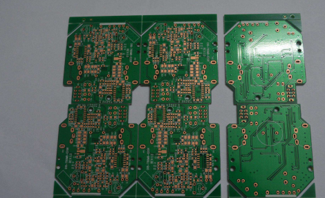
When designing industrial-grade Microtek inverter PCBs, balancing performance with pcb manufacturing cost requires strategic planning. Start by collaborating with experienced pcb manufacturing companies to align your design with industry-grade tolerances and material specifications. For instance, opting for high-Tg FR-4 substrates improves thermal resilience but impacts pcb manufacturing business margins—prioritize designs that minimize waste while meeting IPC Class 3 standards for industrial environments.
Layer stackup optimization is critical. Use symmetrical copper distribution to prevent warping during fabrication, and integrate thermal vias near high-power components like IGBTs or MOSFETs. This reduces hotspots without inflating pcb manufacturing complexity. When selecting surface finishes, HASL-LF offers cost efficiency, but ENIG ensures better solderability for dense layouts—a trade-off that depends on your application’s lifecycle demands.
For trace routing, follow 20% current derating rules to enhance longevity, and maintain clearances compliant with Creepage and Clearance standards. Partnering with pcb manufacturing specialists helps validate designs early, avoiding costly revisions. Finally, implement DFM (Design for Manufacturing) checks to address potential issues like acid traps or uneven copper distribution, ensuring your Microtek PCB aligns with both performance goals and scalable production workflows.
Energy-Efficient Routing Strategies for Inverter Circuits
When designing PCB manufacturing solutions for Microtek inverters, optimizing trace routing is critical to minimizing energy losses and enhancing overall efficiency. Start by prioritizing shorter paths for high-current traces to reduce parasitic resistance, which directly impacts thermal performance and PCB manufacturing cost. Use wider traces in areas with elevated current density, ensuring proper impedance matching to prevent voltage drops.
Collaborating with experienced PCB manufacturing companies ensures adherence to design rules that balance signal integrity and energy conservation. For example, arranging power components closer to their respective drivers reduces loop inductance, a common source of switching losses. Implementing multilayer stacking with dedicated power and ground planes further stabilizes voltage distribution while simplifying routing complexity.
In industrial settings, consider how PCB manufacturing business constraints influence material choices. High-quality substrates with low dielectric loss are essential for minimizing heat generation in high-frequency sections. Additionally, avoid sharp angles in traces to prevent electromagnetic interference (EMI), which can degrade efficiency. Automated routing tools, when calibrated for energy-aware layouts, help maintain consistency while reducing manual errors.
Finally, validate your design through simulation tools to identify hotspots and optimize thermal paths. By integrating these strategies, you ensure that PCB manufacturing cost remains competitive without compromising the inverter’s operational efficiency or longevity.
Conclusion
When designing Microtek inverter PCBs, balancing technical precision with pcb manufacturing cost considerations becomes critical for industrial viability. By focusing on thermal optimization and energy-efficient routing, you ensure the design aligns with both performance targets and budget constraints. Collaborating with experienced pcb manufacturing companies helps bridge the gap between theoretical designs and practical implementation, particularly when addressing challenges like heat dissipation or component longevity.
As you refine your pcb manufacturing business strategies, prioritize partnerships that offer scalable solutions without compromising on material quality or traceability. Advanced cooling systems and robust layout techniques not only enhance reliability but also reduce long-term maintenance expenses—a key factor in sustaining competitiveness. Finally, integrating feedback loops with manufacturers ensures iterative improvements, turning theoretical optimizations into measurable gains for industrial-grade applications.
Frequently Asked Questions
How does thermal management affect PCB manufacturing for Microtek inverters?
Effective thermal design ensures stable operation in industrial environments by preventing component overheating. When working with PCB manufacturing companies, specify materials with high thermal conductivity and consider heat dissipation patterns during layout planning.
What factors influence PCB manufacturing cost in high-power inverter designs?
Costs depend on material quality, layer count, and precision requirements. Industrial-grade designs often require specialized substrates and tight tolerance controls, which PCB manufacturing business partners should address through value engineering without compromising reliability.
How do component selection strategies impact PCB manufacturing timelines?
Choosing industry-certified parts reduces compatibility risks and rework. Collaborate early with your PCB manufacturing companies to validate component footprints and availability, ensuring seamless integration with your Microtek inverter’s power conversion efficiency goals.
Can layout optimization reduce PCB manufacturing cost for complex inverter circuits?
Yes. Strategic component placement minimizes trace lengths and layer transitions, lowering material usage. Use PCB manufacturing design rules to balance density requirements with production feasibility—this becomes critical when scaling for industrial applications.
Ready to Optimize Your Inverter PCB Design?
For tailored solutions that align with these strategies, please click here to connect with specialists experienced in industrial-grade PCB manufacturing business requirements.