Millimeter-Wave PCB Circuit Applications: Design, Challenges, and Future Trends
Abstract
Millimeter-wave (mmWave) frequencies, typically ranging from 30 GHz to 300 GHz, have gained significant attention in modern wireless communication, radar systems, and sensing applications. Printed Circuit Board (PCB) technology plays a crucial role in enabling mmWave circuits due to its cost-effectiveness, scalability, and integration capabilities. This paper explores the key aspects of mmWave PCB design, including material selection, signal integrity, antenna integration, and manufacturing challenges. Furthermore, we discuss emerging applications in 5G/6G communications, automotive radar, and biomedical imaging. Finally, future trends and advancements in mmWave PCB technology are outlined.
1. Introduction
The increasing demand for high-speed data transmission, low-latency communication, and high-resolution sensing has driven the adoption of millimeter-wave (mmWave) frequencies. Unlike traditional microwave bands, mmWave offers wider bandwidths, enabling faster data rates and improved spatial resolution. However, designing PCBs for mmWave applications presents unique challenges, including high propagation losses, stringent signal integrity requirements, and complex electromagnetic interference (EMI) management.
This paper provides a comprehensive overview of mmWave PCB circuit applications, covering design methodologies, material considerations, and implementation challenges. We also highlight key industry applications and future research directions.
2. Fundamentals of Millimeter-Wave PCB Design
2.1 Frequency and Wavelength Considerations
Millimeter-wave signals have wavelengths between 1 mm and 10 mm, leading to several design implications:
- Miniaturization: Components and transmission lines must be extremely compact.
- Skin Effect: At high frequencies, current flows mostly near the conductor surface, increasing resistive losses.
- Dielectric Losses: PCB substrate materials must exhibit low loss tangents to minimize signal attenuation.
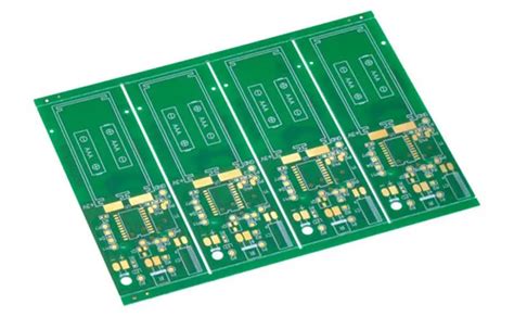
2.2 Key PCB Materials for mmWave Applications
The choice of substrate material significantly impacts performance. Common materials include:
- Rogers RO4000 Series: Low dielectric loss (tan δ ~ 0.0027) and stable permittivity (ε_r ~ 3.38).
- PTFE (Teflon): Excellent high-frequency properties but challenging to manufacture.
- Hydrocarbon Ceramics: Cost-effective with moderate performance.
- Silicon and GaAs: Used in monolithic microwave integrated circuits (MMICs) for hybrid designs.
2.3 Transmission Line Structures
To minimize losses, mmWave PCBs employ specialized transmission lines:
- Microstrip Lines: Simple but suffer from radiation losses at mmWave.
- Coplanar Waveguides (CPW): Provide better shielding and lower dispersion.
- Substrate-Integrated Waveguides (SIW): Mimic traditional waveguides with lower fabrication costs.
3. Signal Integrity and EMI Challenges
3.1 Insertion Loss and Return Loss
- Insertion Loss: Caused by conductor roughness, dielectric absorption, and impedance mismatches.
- Return Loss: Poor impedance matching leads to signal reflections, degrading performance.
3.2 Crosstalk and Radiation Effects
- Crosstalk: High-frequency signals induce unwanted coupling between adjacent traces.
- Radiation Losses: Open microstrip lines can radiate energy, requiring shielding techniques.
3.3 Mitigation Techniques
- Ground Plane Optimization: Proper grounding reduces EMI and improves signal integrity.
- Via Structures: Use of grounded vias to suppress parasitic modes.
- EM Simulation Tools: Advanced software (e.g., HFSS, CST) aids in optimizing layouts.
4. Antenna Integration in mmWave PCBs
Antennas are critical for mmWave systems, and PCB-based designs offer compact solutions:
- Patch Antennas: Widely used due to ease of fabrication and integration.
- Array Antennas: Enable beamforming for 5G and radar applications.
- On-Chip Antennas: Emerging in mmWave System-in-Package (SiP) designs.
5. Key Applications of mmWave PCB Circuits
5.1 5G and 6G Communications
- Massive MIMO: mmWave PCBs enable high-density antenna arrays.
- Beamforming: Phase shifters and RF front-ends integrated on PCBs.
5.2 Automotive Radar (77 GHz and 79 GHz)
- Adaptive Cruise Control (ACC): High-resolution object detection.
- Collision Avoidance: Real-time processing with low-latency PCBs.
5.3 Biomedical Imaging and Sensing
- Non-Invasive Diagnostics: mmWave PCBs used in cancer detection and vital sign monitoring.
- Wearable Sensors: Compact mmWave circuits for health tracking.
5.4 Satellite and Space Communications
- Low Earth Orbit (LEO) Satellites: High-frequency inter-satellite links.
6. Manufacturing and Fabrication Challenges
- Tight Tolerances: Sub-millimeter feature sizes require precision etching.
- Laminate Consistency: Variations in dielectric properties affect performance.
- Assembly Complexity: Flip-chip and wire-bonding techniques for mmWave ICs.
7. Future Trends and Innovations
- AI-Optimized PCB Layouts: Machine learning for automated high-frequency design.
- 3D-Printed mmWave Circuits: Additive manufacturing for rapid prototyping.
- THz (Terahertz) PCBs: Extending beyond 100 GHz for next-gen applications.
8. Conclusion
Millimeter-wave PCB circuits are pivotal in advancing modern wireless technologies. While challenges such as signal loss, EMI, and fabrication precision persist, innovations in materials, simulation tools, and manufacturing techniques continue to push the boundaries. As 5G, automotive radar, and biomedical applications expand, mmWave PCBs will remain a cornerstone of high-frequency electronics.