Miniaturization and integration – on the importance of SIP technology in reducing satellite payload
Miniaturization and integration – on the importance of SIP technology in reducing satellite payload
1.Development of micro-packaging technology
With the requirements of aerospace systems for miniaturization, low power consumption, high performance and high reliability, the shortcomings of the design of traditional PCB board systems (SOB) are becoming more and more obvious. Due to the volume and power consumption limitations of chips and modules, the size and power consumption of PCB boards cannot be reduced indefinitely. The package size of a single chip is usually in the order of mm to cm, but the trace length on the PCB board is usually in the order of 1cm~50cm. Excessive packaging and traces cause large losses and many parasitic parameters, which limit the improvement of system performance. At the same time, due to the complex functions of the system, the use of a large number of discrete devices causes many system failure points and reduces the reliability of the whole machine.
In order to solve the drawbacks of traditional board system design, the aerospace field has gradually begun to adopt micro-packaging and micro-assembly technologies widely used in communications, computers and consumer electronics to improve the integration and reliability of the system.
Typical micro-packaging and micro-assembly technologies include SoC, MCM, SiP, SoP, etc.
SoC technology first appeared in the 1980s. It is used to integrate multiple functional modules into one chip. It is mainly used in high-performance fields such as communications, computers, and networks. Typical examples include NVIDIA’s Tegra, Freescale’s Vybrid, and Intel’s Core series multi-core processors as shown in the figure below. The characteristic of SOC is that multiple functional modules of the same process are integrated into a single chip. It has high system performance and low power consumption. It is the first choice for commercial integrated chip solutions. Its basic requirement is to be implemented on the same semiconductor material, but it is more difficult to achieve in the aerospace field that combines GaAs, GaN and germanium silicon processes.
MCM is also a packaging technology that appeared in the 1980s. Its characteristic is that multiple chips or even bare dies are integrated into one package through gold wire bonding and substrate materials. The size and cost of the module after MCM packaging can be greatly reduced. At the same time, since each chip in the module does not need to be packaged separately and the wiring between chips is shorter, it can provide better transmission performance. In addition, due to the high integration, it is easy to perform centralized shielding and protection, so the system reliability is higher than that of discrete devices. MCM technology can integrate chips of different processes in one package, so it is very flexible to use and can build a hybrid system of analog, digital, RF, and passive devices such as resistors and capacitors. The following figures show two MCM chips developed by IBM and Boeing respectively.
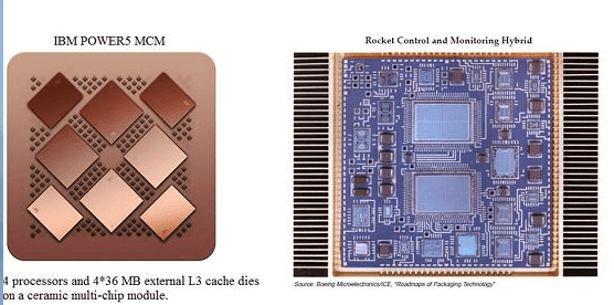
Figure 1 IBM Power5 processor and Boeing’s MCM control chip
SiP is a packaging technology that appeared in the 1990s and can be considered an upgraded version of MCM technology. In addition to being able to perform planar packaging of multiple chips of different processes like MCM, SiP packaging technology can also perform stereoscopic 3D stacking of bare dies or packages, further improving the packaging density. It is currently widely used in portable consumer electronic devices such as mobile phones and PADs, such as the core module of Apple’s iWatch and the T/R module used in phased array radars.
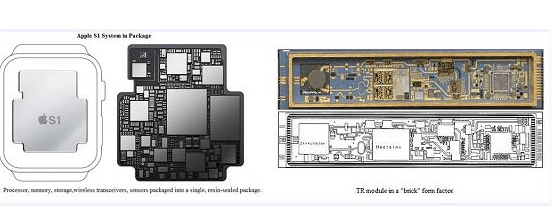
Figure 2 SiP module and RF T/R SiP module used in iWatch
SoP is a packaging technology that appeared at the beginning of this century and can be considered a further upgrade of SiP technology. In addition to being able to complete 3D stacking and packaging of multiple chips and passive devices like SiP, thin film technology and nanomaterials are also used to directly integrate some commonly used passive devices such as resistors, capacitors, filters, waveguides, couplers, antennas and even biosensors onto the package substrate. This reduces the trace length on the substrate from mm to um or even nm, further improving system performance and integration. The following figure is an example of SoP chip application.
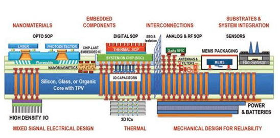
Figure 3 Typical SoP system
It can be seen that SoC, MCM, SiP, SoP and other technologies each have their own characteristics and application areas. In order to achieve the miniaturization of aerospace electronic systems and improve reliability, MCM and SIP are micro-packaging and micro-assembly technologies that can be used in system-level miniaturization design. At the same time, we can focus on the development of SOP technology and make corresponding technical reserves.
2.Challenges of micro-packaging technology
Micro-packaging and micro-assembly technologies can bring significant improvements in integration and system performance, but because they use completely different technologies and processes from traditional board-level system design, their design and testing are very difficult. Especially for high-radiation and high-reliability applications such as space, it is particularly important to conduct reliability design and comprehensive and effective function and performance verification. The main difficulties and challenges of using micro-packaging technology in space applications are reflected in the following aspects.
(1)Design and simulation of micro-packaging materials and interconnection technology: In space applications, the working environment is harsh, such as radiation, temperature, and vibration. The working cycle of a satellite may be more than 20 years and it is almost unrepairable, which makes it very demanding on reliability. Therefore, the selection of packaging materials and interconnection processes is crucial. For substrate materials, there may be a variety of options such as plastics, resins, aluminum, and ceramics; for dielectric materials, BCB (benzocyclobutene) materials, Riston and Kapton materials suitable for harsh environments such as space; for interconnection technology, there may be ball welding, gold wire bonding, silicon through-via (TSV) and other methods, and there are a variety of bonding wire structures for the mainstream gold wire bonding method. Therefore, simulating various material properties, processing technologies, and routing topologies and determining design solutions, while ensuring that the electrical, thermal, and mechanical performance requirements of the space environment are met, has become a difficulty and key technology in system design.
2.Function and performance verification of key chips: Micro-packaged modules package chips with different functions or even bare dies together and bond them together through gold wires. There may be several or even dozens of sub-functional module chips inside the entire module. Since the cost of aerospace-grade chips is very high, if a chip is found to have a problem after packaging, the entire module will be scrapped. Therefore, the detection of chip functions and performance before packaging is crucial to improving the final yield and reducing costs.
3.System function and performance testing of micro-packaged modules: Most micro-packaged modules package two or more functional modules such as analog, RF, digital, power, etc. together with metal or ceramic materials. After the various functional modules are packaged together, the functions and performance of the micro-packaged modules need to be fully tested to ensure that the functions and performance of the packaged modules meet the design requirements. For high-reliability applications, environmental aging tests and screening are also required according to actual work requirements to ensure that they can work reliably and effectively in the next few years or even decades, which makes system function and performance testing of micro-packaged modules crucial.
3.Characterization of key functional modules
(1)Function and performance test of high-speed parallel-to-serial conversion chip
Parallel bus is the earliest and most commonly used bus structure in digital circuits. In order to solve the problem that the parallel bus occupies too large a size and has too stringent requirements on the length of wiring, with the development of chip technology and the increase in speed, more and more digital interfaces have begun to adopt serial bus.
In order to facilitate the transmission of multiple parallel digital signals with as few cables as possible and provide better noise suppression capabilities and transmission distances, multiple parallel data are generally multiplexed together through high-speed TRANSCEIVER chips and transmitted through high-speed low-voltage differential signals.
After the data rate increases, the requirements for impedance matching, line loss and jitter are higher, and signal quality problems are easily caused if you are not careful. The test of high-speed serial transceiver chips mainly involves the following aspects:
·Signal quality test of high-speed serial chip transmitter: including output amplitude, eye diagram, jitter, rise time, fall time, etc.;
·Jitter tolerance, noise tolerance, sensitivity, and system bit error rate test of high-speed serial chip receiver, which are used to verify the bit error rate and receiving tolerance of the actual transmission of the system.
·Chip operating voltage, current, power consumption, etc.
The following is the test platform structure of the entire high-speed transceiver chip transmission system.
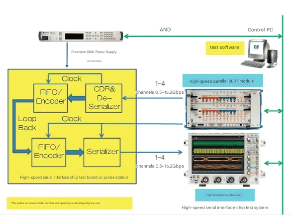
Figure 4
In the test, a high-performance multi-channel bit error meter is used to generate multiple serial excitation signals and clocks to the chip under test. After the data is looped back, it is sent back to the bit error meter for bit error rate statistics or connected to a high-bandwidth oscilloscope for signal quality analysis. During the bit error rate test, random jitter, deterministic jitter, common mode noise, differential mode noise, and ISI inter-symbol interference can be added to the signal to verify the receiver’s tolerance for poor signals.
2.Overall test plan for micro-package modules of electronic systems for satellite camera imaging
The test system should include the following functions.
·CCD signal simulation: It should be able to simulate the analog signal output by the CCD device, and can flexibly add noise to verify the ability of the module under test to extract and restore image data.
·High-speed output data acquisition and analysis: It should be able to acquire and capture the high-speed data output processed by the module under test, and be able to extract image information in the data according to the data structure to verify the function and performance of the module under different working conditions.
·Analysis of analog output signals: measure and analyze the amplitude, frequency, duty cycle, pulse width, etc. of CCD drive clock, motor/shutter and other drive signals.
·Interface control circuit: should be able to control the module to enter normal working state.
·Module power consumption and power supply immunity test: should be able to record the voltage, current, and power consumption of the module under different working conditions, and be able to simulate abnormal conditions such as voltage drop, power supply ripple, and power-on and power-off timing changes to verify the working state of the module under extreme conditions
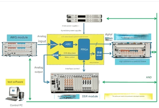
Figure 5: CCD camera SiP module test system
In the test, a high-performance AWG arbitrary waveform generation module is used to simulate the video analog signal output by the CCD, which is output in high-speed digital form after being collected and processed by the module under test. If it is parallel data capture, high-speed parallel data can be captured and analyzed with a high-speed logic analyzer module; if it is multi-channel high-speed serial data, the input end of the parallel bit error meter can be used for clock recovery and data capture. The test requires that the AWG module’s signal-to-noise ratio, dynamic range, bandwidth and other indicators can meet the system’s signal-to-noise ratio test requirements, can flexibly add interference factors such as noise, and have deep enough memory to generate the signal of the entire video frame. The logic analyzer should have a high enough state sampling rate and memory depth, and the bit error tester should have multi-channel serial data input capabilities, clock recovery capabilities, high-speed signal equalization capabilities and sufficient memory depth.


