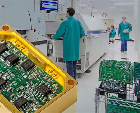
Modern PCB Assembly Machinery: Enhancing Production Efficiency
Key Takeaways
Modern PCB assembly processes rely on three core innovations: automated placement systems, precision soldering technologies, and AI-driven inspection tools. These advancements collectively optimize throughput while minimizing defects, making PCBA (Printed Circuit Board Assembly) workflows more efficient than traditional methods.
| Technology | Impact on Efficiency | Defect Reduction |
|---|---|---|
| Automated Pick-and-Place | 40-60% faster placement | 25% fewer misalignments |
| Laser Soldering Systems | ±5μm precision | 30% lower solder defects |
| AI Visual Inspection | 99.9% detection accuracy | 50% fewer rework cycles |
Tip: To maximize ROI, manufacturers should prioritize integrating AI-driven inspection with existing PCBA lines, as real-time defect detection minimizes downtime.
Transitioning from manual to automated PCB assembly reduces human error, particularly in high-volume production. For instance, surface-mount technology (SMT) machines now handle components as small as 01005 packages, ensuring consistent placement accuracy. Meanwhile, reflow ovens with closed-loop thermal profiling maintain solder joint integrity across diverse board designs.
The synergy between automated optical inspection (AOI) and machine learning algorithms enables predictive maintenance, further streamlining electronics manufacturing. By adopting these technologies, companies achieve faster time-to-market while adhering to stringent quality standards.
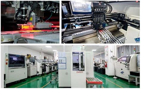
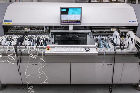
Automated PCB Placement Systems Guide
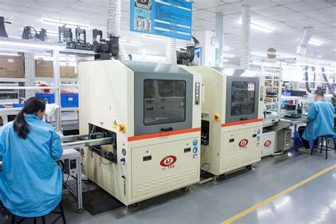
At the core of modern PCB assembly workflows, automated placement systems have revolutionized how components are mounted onto boards. These systems leverage high-speed pick-and-place machines, capable of positioning thousands of surface-mount devices (SMDs) per hour with sub-4-micron accuracy. By integrating advanced vision systems and AI-powered alignment algorithms, they minimize human error while adapting to diverse PCBA designs—from simple single-layer boards to complex multi-chip modules.
A critical advantage lies in their ability to handle microscopic components, such as 0201 resistors or ultra-fine-pitch BGAs, which manual processes struggle to manage consistently. Modern machines also feature dynamic feeder systems that automatically adjust component reels, reducing downtime during product changeovers. This flexibility is vital for manufacturers balancing high-mix, low-volume orders with mass production demands.
Furthermore, real-time data analytics embedded within these systems enable predictive maintenance, identifying potential nozzle wear or calibration drift before defects occur. When paired with automated optical inspection (AOI), the entire placement process becomes a closed-loop quality control mechanism. Such integration not only accelerates throughput but also ensures compliance with stringent industry standards like IPC-A-610.
The shift toward smart manufacturing has further enhanced these systems’ capabilities. Machine learning algorithms now optimize component sequencing and placement paths, trimming cycle times by up to 15%. For PCB assembly facilities, this translates to faster time-to-market and improved ROI—key drivers in today’s competitive electronics landscape.
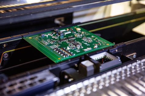
Precision Soldering Tech Advancements
The evolution of precision soldering technology has become a cornerstone in modern PCB assembly workflows, addressing the growing demand for miniaturization and higher component density. Traditional soldering methods, such as wave soldering and reflow ovens, have been enhanced with closed-loop thermal control systems to maintain consistent temperature profiles across complex PCBA designs. Innovations like laser soldering now enable micron-level accuracy, particularly for fine-pitch components and high-density interconnect (HDI) boards, reducing the risk of bridging or cold joints.
Advanced solder paste formulations, including lead-free alloys and low-voiding pastes, further optimize joint reliability while complying with environmental regulations. Integrated automated optical inspection (AOI) systems work in tandem with soldering equipment to detect anomalies in real time, ensuring defects are flagged before downstream processes. Additionally, vapor phase reflow technology has gained traction for its uniform heat distribution, minimizing thermal stress on sensitive components.
This shift toward data-driven soldering processes—powered by IoT-enabled monitoring—allows manufacturers to fine-tune parameters like temperature gradients and dwell times dynamically. Such advancements not only boost throughput in PCB assembly lines but also align with the broader industry goal of zero-defect manufacturing, reinforcing the role of precision soldering as a critical enabler in next-generation electronics production.
AI-Driven Inspection for PCB Quality
The integration of AI-driven inspection systems has revolutionized quality control in PCB assembly processes. By leveraging machine learning algorithms and high-resolution imaging, these systems analyze solder joints, component alignment, and trace integrity with unparalleled accuracy. Unlike traditional manual checks, AI-powered tools detect microscopic defects—such as cold solder joints or misaligned capacitors—in real time, reducing human error and accelerating inspection cycles.
In PCBA workflows, predictive analytics enable these systems to learn from historical data, continuously improving defect detection rates. For instance, AI models trained on thousands of circuit board images can identify subtle anomalies that might escape even experienced technicians. This capability not only minimizes rework but also ensures compliance with stringent industry standards.
Moreover, AI inspection tools seamlessly integrate with automated placement systems and precision soldering technologies, creating a cohesive production line. By flagging issues early, they prevent defective boards from advancing to subsequent stages, optimizing resource utilization. Manufacturers report up to a 30% reduction in defects when deploying these systems, alongside faster time-to-market for complex electronics.
As PCB assembly equipment evolves, the synergy between AI and real-time analytics is setting new benchmarks for reliability. This advancement underscores the shift toward smarter, data-driven manufacturing ecosystems in the electronics industry.
Enhancing Efficiency in PCB Assembly
The drive to optimize PCB assembly processes hinges on integrating next-generation machinery that minimizes human intervention while maximizing output consistency. Central to this evolution are automated pick-and-place systems, which achieve placement accuracies within microns, reducing manual errors by over 70% in PCBA workflows. These systems work in tandem with adaptive conveyor mechanisms that dynamically adjust throughput based on real-time production demands, ensuring seamless material flow.
Another critical factor is the adoption of precision soldering technologies, such as laser-assisted reflow ovens, which maintain exact temperature profiles for diverse component types. This eliminates thermal stress risks, a common defect source in traditional PCB assembly lines. Additionally, AI-powered optical inspection tools scan boards at speeds exceeding 10,000 components per hour, flagging micro-scale anomalies—like solder bridging or misalignments—before they escalate.
By unifying these advancements, manufacturers achieve holistic efficiency gains: shorter cycle times, higher first-pass yields, and reduced rework costs. Industry reports indicate facilities leveraging such integrated systems experience up to 40% faster time-to-market for complex PCBA projects, underscoring the transformative role of modern equipment in electronics manufacturing.
Modern Machinery for Electronics Production
The evolution of PCB assembly technologies has redefined electronics manufacturing, enabling faster, more accurate, and scalable production processes. Central to this transformation are automated pick-and-place systems, which utilize high-speed robotics to position components on circuit boards with micron-level precision. These systems, integrated with PCBA workflows, minimize human error while handling complex designs, from multilayer boards to micro-BGA packages.
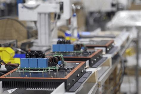
Advancements in modular machinery architectures allow manufacturers to adapt quickly to changing product demands. For instance, modern PCB assembly lines now combine solder paste printers, reflow ovens, and inspection modules into seamless, interconnected units. This integration reduces downtime and supports just-in-time manufacturing principles, critical for industries like automotive and IoT device production.
Another breakthrough lies in real-time process monitoring, where sensors collect data on temperature, alignment, and solder joint quality. By analyzing this data, PCBA systems automatically adjust parameters to maintain consistency across batches—a vital feature for achieving zero-defect manufacturing targets. Such innovations not only enhance throughput but also align with sustainability goals by reducing material waste.
As production scales, the role of interoperable software platforms becomes pivotal. These systems unify design files, machine instructions, and quality logs, ensuring traceability from prototype to mass production. For electronics manufacturers, investing in modern PCB assembly machinery is no longer optional but a strategic imperative to meet global demand while adhering to Industry 4.0 standards.
Reducing Defects With Automated Tools
The integration of automated tools in PCB assembly processes has become pivotal in minimizing production errors and ensuring consistent quality. Advanced systems like automated optical inspection (AOI) and X-ray inspection enable real-time detection of soldering defects, component misalignment, or micro-cracks that manual checks might overlook. These tools leverage high-resolution imaging and AI-driven algorithms to analyze thousands of connections per minute, reducing human error by over 60% in typical PCBA workflows.
Furthermore, closed-loop feedback mechanisms in modern assembly lines automatically adjust parameters such as solder paste deposition or placement pressure, correcting deviations before they escalate into costly rework. For instance, precision dispensers equipped with laser-guided calibration ensure micron-level accuracy, critical for high-density interconnect (HDI) boards. By pairing automated tools with predictive analytics, manufacturers can identify patterns in defect occurrence, enabling proactive maintenance of PCB assembly equipment. This not only slashes defect rates but also extends machinery lifespan, aligning with lean manufacturing principles.
As manufacturers adopt these innovations, the synergy between PCBA automation and data-driven decision-making continues to redefine quality benchmarks, ensuring faster time-to-market without compromising reliability.
Streamlining Manufacturing Through AI Tech
The integration of AI-driven systems into PCB assembly workflows has revolutionized quality control and process optimization. By leveraging machine learning algorithms, manufacturers can now analyze vast datasets from PCBA production lines to identify patterns that human operators might overlook. For instance, real-time defect detection tools powered by AI scan solder joints, component placements, and trace alignments at speeds exceeding 50,000 inspections per hour, slashing error rates by up to 65% compared to manual checks.
Advanced PCB assembly equipment now embeds predictive maintenance capabilities, where AI models monitor motor vibrations, temperature fluctuations, and wear patterns in pick-and-place machines. This proactive approach reduces unplanned downtime by 30–40%, ensuring consistent throughput. Furthermore, AI optimizes material utilization by dynamically adjusting stencil pressure and solder paste volume based on component-specific requirements, minimizing waste without compromising joint reliability.
Transitioning seamlessly from precision soldering advancements, these intelligent systems also enhance traceability. Every PCBA unit receives a digital fingerprint, allowing manufacturers to trace defects back to specific process stages. As production scales, AI’s adaptive learning ensures continuous improvement, making it indispensable for meeting today’s demands for high-volume, zero-defect electronics manufacturing.
Key Trends in PCB Assembly Equipment
The pcb assembly landscape is evolving rapidly, driven by demands for higher precision and faster production cycles. A dominant trend is the integration of modular automation in pcba workflows, enabling manufacturers to reconfigure assembly lines dynamically for diverse product batches. Advanced automated optical inspection (AOI) systems now leverage machine learning algorithms to detect micron-level defects, reducing manual intervention by over 40%.
Another notable development is the adoption of hybrid soldering technologies, combining laser-assisted processes with convection reflow to handle delicate components in high-density pcb assembly. This approach minimizes thermal stress, critical for applications like automotive electronics. Meanwhile, cloud-connected machinery is gaining traction, allowing real-time monitoring of pcba production metrics across global facilities.
Sustainability is also reshaping equipment design, with energy-efficient pick-and-place systems cutting power consumption by up to 25%. Additionally, collaborative robots (cobots) are being deployed alongside human operators for tasks like component feeding, enhancing throughput without compromising flexibility. These innovations underscore a broader shift toward smart manufacturing ecosystems in pcb assembly, where data-driven decisions and interoperability between tools define next-gen production efficiency.
Conclusion
The evolution of PCB assembly technologies has redefined modern electronics manufacturing, enabling unprecedented levels of precision and efficiency. By integrating automated placement systems and AI-driven inspection tools, manufacturers can now achieve PCBA workflows that minimize human error while maximizing throughput. Advanced solder paste inspection (SPI) systems and reflow profiling techniques ensure consistent joint quality, directly addressing the industry’s demand for zero-defect manufacturing. Furthermore, the adoption of machine learning algorithms in defect detection not only accelerates production cycles but also reduces material waste, aligning with sustainable practices.
As the complexity of electronic devices grows, the role of PCB assembly equipment becomes increasingly critical. Innovations like closed-loop feedback systems and predictive maintenance modules are setting new benchmarks for operational reliability. These advancements underscore a clear trajectory: the fusion of PCBA automation with intelligent data analytics is no longer optional but a strategic imperative for staying competitive. By prioritizing scalable, adaptable machinery, manufacturers can future-proof their operations against rapidly shifting market demands while maintaining rigorous quality standards.
Frequently Asked Questions
How does automation improve accuracy in PCB assembly processes?
Automated PCB assembly systems utilize robotic placement arms and vision-guided alignment to achieve micron-level precision. These systems reduce human error, ensuring components like microchips and resistors are positioned correctly, which directly enhances PCBA quality and yield rates.
What advancements in soldering technology benefit modern electronics manufacturing?
Modern PCB assembly lines employ laser soldering and reflow ovens with closed-loop thermal control. These technologies maintain consistent heat profiles, minimizing cold joints or bridging. Such precision is critical for high-density PCBA designs found in wearables and IoT devices.
Can AI-driven inspection tools detect defects that traditional methods miss?
Yes. AI-powered optical inspection (AOI) systems analyze solder joints, component alignment, and trace integrity using machine learning algorithms. These tools identify microscopic flaws or pattern deviations that human inspectors might overlook, reducing defect rates by up to 30% in PCBA workflows.
How do modular equipment designs impact production scalability?
Modular PCB assembly machines allow manufacturers to reconfigure lines quickly for different product batches. This flexibility supports mixed-volume production, enabling seamless transitions between prototyping and mass manufacturing without significant downtime.
Ready to Optimize Your PCB Assembly Process?
For tailored solutions in advanced PCB assembly equipment, please click here to explore how our technologies can elevate your production efficiency and product reliability.


