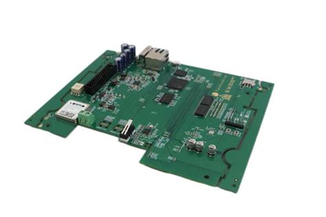
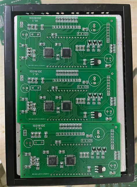
Mounting components on pcb
Surface Mount Technology: Techniques and Best Practices
Surface Mount Technology (SMT) has revolutionized the electronics manufacturing industry by enabling the production of smaller, more efficient, and highly reliable electronic devices. This technology involves mounting components directly onto the surface of printed circuit boards (PCBs), eliminating the need for drilling holes as required in through-hole technology. As the demand for compact and complex electronic devices continues to grow, understanding the techniques and best practices for mounting components on PCBs using SMT becomes increasingly important.
To begin with, the SMT process involves several critical steps, each requiring precision and attention to detail.
The first step is the application of solder paste onto the PCB. This is typically achieved using a stencil that matches the layout of the PCB, ensuring that the solder paste is applied only to the designated pads. The quality of the solder paste and its application is crucial, as it serves as the adhesive that holds the components in place and provides the electrical connection between the components and the PCB.
Following the application of solder paste, the next step is the placement of components.
This is usually performed by automated pick-and-place machines, which are capable of placing thousands of components per hour with high accuracy. These machines use vision systems to ensure that each component is correctly oriented and positioned on the PCB. The precision of component placement is vital, as even slight misalignments can lead to defects such as tombstoning or insufficient solder joints.
Once the components are placed, the assembly is subjected to a reflow soldering process.
During reflow, the assembly is passed through a controlled heat profile in a reflow oven, causing the solder paste to melt and form solid solder joints as it cools. The reflow process must be carefully controlled to prevent defects such as solder bridging or voids, which can compromise the functionality and reliability of the final product.
In addition to these core steps, several best practices can enhance the quality and efficiency of SMT.
One such practice is the use of design for manufacturability (DFM) principles during the PCB design phase. By considering factors such as component spacing, pad design, and thermal management, designers can create PCBs that are easier to manufacture and less prone to defects. Furthermore, regular inspection and testing throughout the SMT process are essential to identify and rectify any issues early on. Techniques such as automated optical inspection (AOI) and X-ray inspection can detect defects that are not visible to the naked eye, ensuring that only high-quality assemblies proceed to the next stage of production.
Moreover, the choice of materials and equipment plays a significant role in the success of SMT.
High-quality solder paste, reliable pick-and-place machines, and well-maintained reflow ovens contribute to consistent and defect-free assemblies. Additionally, ongoing training and skill development for personnel involved in the SMT process can lead to improved performance and reduced error rates.
In conclusion, Surface Mount Technology is a cornerstone of modern electronics manufacturing, offering numerous advantages in terms of size, weight, and performance. By adhering to established techniques and best practices, manufacturers can optimize their SMT processes, resulting in high-quality, reliable electronic products. As technology continues to evolve, staying informed about the latest advancements and methodologies in SMT will be crucial for maintaining a competitive edge in the industry.
Through-Hole Mounting: Advantages and Applications
Through-hole mounting, a traditional method of attaching components to printed circuit boards (PCBs), remains a vital technique in the electronics industry despite the advent of surface-mount technology. This method involves inserting component leads through pre-drilled holes on the PCB and soldering them to pads on the opposite side. While surface-mount technology offers advantages in terms of size and automation, through-hole mounting continues to be favored in specific applications due to its unique benefits.
One of the primary advantages of through-hole mounting is its mechanical strength.
Components mounted using this method are secured by their leads, which pass through the board, providing a robust physical connection. This makes through-hole mounting particularly suitable for applications where the PCB may be subject to mechanical stress or vibration. For instance, in automotive and aerospace industries, where reliability under harsh conditions is paramount, through-hole components are often preferred. The secure attachment ensures that components remain in place, reducing the risk of failure due to physical disturbances.
Moreover, through-hole mounting facilitates easier manual assembly and prototyping.
Engineers and hobbyists alike appreciate the simplicity of inserting components by hand, which allows for quick modifications and testing during the development phase. This ease of use is particularly beneficial in educational settings, where students can gain hands-on experience with electronic components without the need for specialized equipment. Additionally, through-hole components are generally larger and easier to handle, making them ideal for those new to electronics or working on projects that do not require miniaturization.
In terms of thermal performance, through-hole mounting offers distinct advantages.
The leads of through-hole components can act as heat sinks, dissipating heat away from the component body and into the PCB. This can be crucial in high-power applications where effective heat management is necessary to prevent component failure. Furthermore, the larger size of through-hole components often allows for better heat dissipation compared to their surface-mount counterparts, which can be critical in maintaining the longevity and reliability of electronic devices.
Despite these advantages, it is important to acknowledge the limitations of through-hole mounting.
The need for drilling holes in the PCB can increase manufacturing complexity and cost. Additionally, through-hole components typically occupy more space on the board, which can be a disadvantage in applications where compactness is essential. However, these drawbacks are often outweighed by the benefits in scenarios where durability and ease of assembly are prioritized.
Through-hole mounting also finds applications in power electronics and high-voltage circuits.
The physical separation provided by the PCB can help in managing electrical isolation and reducing the risk of short circuits. This is particularly important in power supplies and amplifiers, where high voltages and currents are present. The ability to handle higher power levels makes through-hole components a preferred choice in these applications.
In conclusion, while surface-mount technology has become the standard for many modern electronic devices, through-hole mounting continues to play a crucial role in the industry. Its mechanical strength, ease of assembly, and thermal performance make it an indispensable technique in various applications. As technology advances, the coexistence of through-hole and surface-mount technologies ensures that engineers have the flexibility to choose the most appropriate method for their specific needs, balancing the trade-offs between size, cost, and performance.
Mixed Technology PCB Assembly: Combining SMT and Through-Hole
In the realm of electronics manufacturing, the assembly of printed circuit boards (PCBs) is a critical process that demands precision and expertise. Among the various techniques employed, mixed technology PCB assembly stands out as a sophisticated method that combines Surface Mount Technology (SMT) and through-hole technology. This approach leverages the advantages of both techniques, allowing for the creation of complex and highly functional electronic devices. Understanding the nuances of mixed technology PCB assembly is essential for those involved in the design and production of modern electronic components.
Surface Mount Technology (SMT) has revolutionized the electronics industry by enabling the placement of components directly onto the surface of the PCB.
This method offers several benefits, including reduced size and weight of the final product, increased component density, and improved performance due to shorter electrical paths. SMT components are typically smaller and lighter, which allows for more compact and efficient designs. However, despite these advantages, SMT is not without its limitations. Certain components, such as connectors and large capacitors, may not be suitable for surface mounting due to their size or mechanical requirements.
On the other hand, through-hole technology involves inserting component leads through pre-drilled holes in the PCB and soldering them on the opposite side.
This method provides robust mechanical bonds, making it ideal for components that require additional support or are subject to mechanical stress. Through-hole technology is also preferred for components that need to handle high power or high voltage, as the leads can dissipate heat more effectively. Nevertheless, through-hole assembly is generally more labor-intensive and less suitable for high-density applications compared to SMT.
The integration of SMT and through-hole technologies in mixed technology PCB assembly allows manufacturers to capitalize on the strengths of both methods.
By strategically selecting which components to mount using SMT and which to use through-hole, designers can optimize the performance, reliability, and cost-effectiveness of the final product. For instance, critical components that require strong mechanical support or are subject to frequent insertion and removal can be mounted using through-hole technology, while smaller, less critical components can be placed using SMT to save space and reduce weight.
Transitioning between SMT and through-hole assembly within a single PCB requires careful planning and coordination.
The design phase must account for the different requirements of each technology, such as pad sizes, hole diameters, and soldering techniques. Additionally, the assembly process must be meticulously organized to ensure that each component is mounted correctly and that the integrity of the PCB is maintained. This often involves using specialized equipment and techniques, such as reflow soldering for SMT components and wave soldering for through-hole components.
In conclusion, mixed technology PCB assembly represents a sophisticated approach to electronic manufacturing that combines the best of both SMT and through-hole technologies. By understanding the unique advantages and limitations of each method, manufacturers can create highly functional and reliable electronic devices that meet the demands of modern applications. As technology continues to evolve, the ability to effectively integrate these two assembly techniques will remain a valuable skill in the electronics industry, driving innovation and enabling the development of increasingly complex and capable devices.
Automated vs. Manual PCB Assembly: Choosing the Right Method
In the realm of electronics manufacturing, the process of mounting components on a printed circuit board (PCB) is a critical step that can significantly influence the performance and reliability of the final product. As technology advances, manufacturers are faced with the decision of choosing between automated and manual PCB assembly methods. Each approach has its own set of advantages and limitations, making it essential to understand the nuances of both to make an informed decision.
Automated PCB assembly, often referred to as surface mount technology (SMT), has become increasingly popular due to its efficiency and precision.
This method employs sophisticated machinery to place components onto the PCB with remarkable accuracy. One of the primary benefits of automated assembly is its ability to handle high-volume production runs with consistent quality. The use of automated systems reduces the likelihood of human error, ensuring that each board is assembled to exact specifications. Moreover, automated assembly can accommodate a wide range of component sizes and types, making it a versatile option for complex designs.
In addition to precision and efficiency, automated assembly offers significant time savings.
The speed at which machines can place components far surpasses that of manual assembly, allowing manufacturers to meet tight deadlines and increase throughput. Furthermore, the repeatability of automated processes ensures that each PCB is identical, which is crucial for maintaining product consistency and reliability. However, it is important to note that the initial setup costs for automated assembly can be substantial, as it requires investment in specialized equipment and programming.
On the other hand, manual PCB assembly, also known as through-hole technology (THT), remains a viable option for certain applications.
This method involves skilled technicians manually placing and soldering components onto the PCB. While manual assembly is generally slower and more labor-intensive than automated methods, it offers distinct advantages in specific scenarios. For instance, manual assembly is particularly well-suited for prototypes and small production runs where the cost of setting up automated equipment may not be justified. Additionally, manual assembly allows for greater flexibility in design changes, as technicians can easily adapt to modifications without the need for reprogramming machinery.
Moreover, manual assembly is often preferred for components that are not compatible with automated systems, such as large connectors or components with irregular shapes. The tactile feedback and visual inspection provided by skilled technicians can also be beneficial in identifying and addressing potential issues during the assembly process. However, the reliance on human labor introduces variability, which can impact the consistency and quality of the final product.
In conclusion, the choice between automated and manual PCB assembly depends on various factors, including production volume, budget, and design complexity.
Automated assembly is ideal for high-volume production with stringent quality requirements, offering speed, precision, and consistency. Conversely, manual assembly provides flexibility and adaptability, making it suitable for prototypes, small batches, and unique component requirements. Ultimately, manufacturers must carefully evaluate their specific needs and constraints to determine the most appropriate method for mounting components on PCBs. By understanding the strengths and limitations of each approach, manufacturers can optimize their assembly processes and ensure the successful production of reliable electronic devices.


