MPI PCB Maker: Advanced Materials for High-Speed PCBs

Key Takeaways
When exploring PCB manufacturing for high-frequency applications, you’ll find that MPI materials redefine performance benchmarks. Unlike traditional polyimide (PI) substrates, modified polyimide offers enhanced dielectric stability, critical for minimizing signal loss in 5G/6G systems. For PCB manufacturing companies, this translates to improved thermal management—key for maintaining reliability in compact mobile devices where heat dissipation challenges escalate.
Tip: When selecting materials for high-speed designs, prioritize dielectric properties and thermal resistance to balance PCB manufacturing cost and long-term performance.
The shift to MPI-based solutions also impacts PCB manufacturing business strategies. By reducing impedance variations and supporting finer trace geometries, these materials enable tighter integration in RF modules and antenna arrays. This is particularly valuable for applications like millimeter-wave communications, where even minor signal degradation can compromise system efficiency.
For engineers, MPI’s low-loss characteristics simplify achieving compliance with stringent RF measurement standards. Whether optimizing probe systems or designing flex circuits, the material’s stability across temperature fluctuations ensures consistent results—a decisive factor in next-gen communication hardware. By integrating MPI, you’re not just upgrading materials; you’re future-proofing designs against evolving technical demands.
MPI Materials Revolutionize High-Speed PCB Design
When designing high-frequency circuits for 5G infrastructure or advanced mobile devices, PCB manufacturing companies face critical challenges in balancing thermal performance and signal integrity. Modified polyimide (MPI) materials address these demands by offering ultra-low dielectric loss and enhanced thermal stability, enabling circuits to maintain consistent performance even under extreme operating conditions. Unlike traditional FR-4 or standard polyimide substrates, MPI’s unique molecular structure reduces signal distortion at frequencies above 10 GHz, a necessity for next-gen communication systems.
For PCB manufacturing businesses, adopting MPI translates to reduced PCB manufacturing cost over time. While initial material expenses may be higher, MPI’s durability minimizes rework rates and extends product lifespans—key factors in high-reliability applications like aerospace or automotive radar systems. Engineers leveraging MPI can also achieve thinner trace widths without sacrificing impedance control, unlocking compact designs for wearables and IoT devices.
By integrating MPI into PCB manufacturing workflows, you gain a competitive edge in markets prioritizing miniaturization and energy efficiency. Its compatibility with hybrid stacking techniques further simplifies transitions from legacy materials, ensuring seamless scalability for future high-speed projects.
Modified Polyimide Solutions for 5G/6G Systems
When designing high-frequency circuits for 5G/6G systems, PCB manufacturing companies face unique challenges in balancing thermal performance, signal integrity, and material reliability. Modified polyimide (MPI) solutions address these demands by offering ultra-low dielectric loss and enhanced thermal conductivity, critical for minimizing energy dissipation in densely packed mobile devices. Unlike traditional materials, MPI maintains stable electrical properties even under extreme temperature fluctuations—a non-negotiable feature for PCB manufacturing in next-gen communication infrastructure.
For PCB manufacturing businesses, adopting MPI translates to improved yield rates and reduced PCB manufacturing cost over time. This is achieved through MPI’s compatibility with high-speed lamination processes and resistance to warping during multilayer stacking. Below is a comparison of MPI’s performance against conventional polyimide (PI) in key areas:
| Property | MPI | Traditional PI |
|---|---|---|
| Dielectric Constant (Dk) | 3.2 @ 10 GHz | 3.5 @ 10 GHz |
| Loss Tangent (Df) | 0.002 | 0.0035 |
| Thermal Conductivity | 0.45 W/mK | 0.25 W/mK |
| Glass Transition Temp | >280°C | 220°C |
By leveraging MPI’s high-frequency stability, engineers can achieve tighter impedance control in RF circuits, reducing signal distortion in millimeter-wave applications. This makes MPI indispensable for PCB manufacturing in phased-array antennas and low-latency network equipment. As 5G evolves toward 6G, selecting materials that support terahertz frequencies while maintaining mechanical durability becomes pivotal—a gap MPI fills effectively.
Superior Thermal Stability in MPI PCB Manufacturing
When selecting materials for PCB manufacturing, thermal stability becomes particularly crucial for high-speed applications. Modified polyimide (MPI) substrates excel in maintaining structural integrity across temperature fluctuations ranging from -65°C to 260°C, a critical advantage for PCB manufacturing companies designing boards for 5G infrastructure or aerospace systems. Unlike conventional polyimide materials, MPI’s low coefficient of thermal expansion (CTE) minimizes warping during soldering processes, reducing defects in multi-layer designs.
This thermal resilience directly impacts PCB manufacturing cost by lowering scrap rates and improving yield consistency. For instance, MPI’s ability to withstand repeated thermal cycling reduces the risk of delamination in high-power RF circuits—a common failure mode in traditional FR-4 or standard polyimide boards. Additionally, the material’s inherent heat dissipation properties enable denser component layouts without compromising reliability, a key consideration for PCB manufacturing business models prioritizing miniaturized, high-performance designs.
By integrating MPI substrates, manufacturers achieve tighter impedance control even under extreme operating conditions, ensuring stable signal transmission in millimeter-wave applications. This thermal performance also extends the lifespan of high-frequency circuits, aligning with the durability demands of next-gen communication systems. Transitioning to MPI materials allows engineers to balance thermal management with signal integrity—a dual challenge in modern PCB manufacturing workflows.
High-Frequency Performance in Mobile Device PCBs
When designing mobile devices for 5G/6G applications, maintaining high-frequency performance becomes critical. Modern smartphones and wearables demand PCBs that minimize signal loss while handling millimeter-wave frequencies. This is where MPI PCB Maker’s modified polyimide materials excel, offering ultra-low dielectric loss and consistent impedance control even in compact layouts. For PCB manufacturing companies, these properties simplify the production of multi-layer boards with tighter tolerances, reducing the risk of performance degradation in high-speed circuits.
Balancing PCB manufacturing cost with performance is a key challenge. Traditional materials often require additional shielding or complex layouts to mitigate interference, driving up expenses. MPI’s thermally stable substrates eliminate the need for such compromises, enabling leaner designs without sacrificing signal integrity. As mobile devices shrink in size, the PCB manufacturing business increasingly prioritizes materials that support thinner traces and higher component density—both areas where MPI’s solutions outperform conventional options.
By integrating these advanced materials, you can achieve enhanced power efficiency and reduced heat generation, critical for prolonging battery life in portable electronics. Whether optimizing antenna modules or RF front-end circuits, MPI’s technology ensures your designs meet the rigorous demands of next-gen connectivity while streamlining PCB manufacturing workflows.
MPI Flex Circuits vs Traditional PI Materials
When choosing between MPI flex circuits and conventional polyimide (PI) materials, you’ll notice critical differences in performance and application. Traditional PI has long been the backbone of flexible PCB manufacturing, offering decent thermal resistance and mechanical durability. However, MPI’s modified polyimide formulation introduces enhanced high-frequency stability—a game-changer for 5G/6G systems and compact mobile devices where signal integrity is non-negotiable.
For PCB manufacturing companies, MPI’s lower dielectric loss at millimeter-wave frequencies reduces signal degradation, enabling thinner, lighter designs without sacrificing reliability. This advantage becomes critical when balancing PCB manufacturing cost with performance demands—especially in high-volume production for aerospace or IoT applications. While traditional PI materials may still suffice for simpler circuits, MPI’s thermal expansion coefficient aligns better with copper layers, minimizing delamination risks during rapid temperature cycling.
If you’re managing a PCB manufacturing business, transitioning to MPI requires evaluating material compatibility and process adjustments. Though initial costs might rise, the long-term benefits—like reduced rework rates and compatibility with advanced RF probe systems—can offset upfront investments. By prioritizing MPI for high-speed designs, you position your offerings at the forefront of innovation while addressing evolving industry standards.
Signal Integrity Advancements with MPI Technology
When designing high-frequency circuits, maintaining signal integrity becomes critical as data rates push beyond 100 Gbps in 5G/6G systems. MPI technology addresses this challenge by leveraging modified polyimide materials with ultra-low dielectric loss (Df < 0.002 at 10 GHz), minimizing signal distortion across traces. Unlike traditional PCB manufacturing approaches using FR-4 or standard polyimide, MPI’s homogeneous dielectric properties reduce impedance mismatches, ensuring consistent performance even in dense, multilayer designs.
For PCB manufacturing companies, this translates to fewer post-production revisions. By integrating MPI materials early in the PCB manufacturing business workflow, you eliminate the need for costly impedance-tuning steps, directly reducing PCB manufacturing cost while boosting yield rates. The material’s thermal stability (Tg > 260°C) further prevents warping during reflow processes, preserving signal paths in high-speed applications like millimeter-wave antennas or server backplanes.
Advanced simulation tools paired with MPI substrates allow engineers to predict signal behavior with ±5% accuracy, enabling first-pass success in RF-heavy designs. Whether you’re prototyping for IoT modules or scaling production for automotive radar systems, MPI’s balanced dielectric constant (Dk 3.2±0.05) ensures minimal crosstalk and attenuation—key factors in maintaining edge rates for next-gen communication hardware.
MPI PCB Applications in Next-Gen Communication
When designing PCB manufacturing solutions for next-generation communication systems, MPI materials offer critical advantages in balancing signal integrity and thermal demands. As 5G/6G networks require faster data transmission and reduced latency, PCB manufacturing companies must prioritize substrates that minimize signal loss at millimeter-wave frequencies. Modified polyimide (MPI) achieves this by maintaining consistent dielectric properties across wide temperature ranges, ensuring stable performance in base stations, satellite communication modules, and advanced mobile devices.
For PCB manufacturing business stakeholders, MPI’s compatibility with high-density interconnect (HDI) designs reduces layer counts while maintaining impedance control—a key factor in lowering PCB manufacturing cost for complex RF boards. Its low dissipation factor (Df) of ≤0.002 at 10 GHz outperforms traditional FR-4 and even some high-frequency laminates, enabling tighter trace spacing without compromising signal fidelity. This makes MPI ideal for phased-array antennas and beamforming circuits, where precise timing alignment is non-negotiable.
By integrating MPI into your PCB manufacturing workflows, you gain a material platform that supports both rigid and flex configurations, future-proofing designs against evolving network standards. Its resistance to thermal expansion also enhances reliability in outdoor infrastructure, where temperature fluctuations can degrade conventional substrates over time.
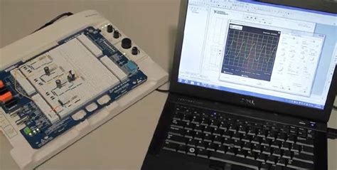
Optimizing RF Measurements via MPI Probe Systems
When working with high-frequency circuits in PCB manufacturing, achieving precise RF measurements requires specialized tools that minimize signal distortion. MPI probe systems address this challenge by integrating impedance-matched contact points and low-loss dielectric interfaces specifically engineered for multi-gigahertz applications. Unlike conventional probing methods that introduce parasitic capacitance, these systems maintain signal integrity through controlled impedance paths—critical for validating designs in 5G/6G infrastructure and millimeter-wave devices.
For PCB manufacturing companies, adopting MPI probe technology directly impacts PCB manufacturing cost by reducing retest rates caused by measurement inaccuracies. The probes’ thermal-stable construction ensures consistent performance across temperature fluctuations, a key advantage for high-power RF boards used in base stations. Additionally, their compatibility with automated test equipment (ATE) streamlines production workflows, enabling faster throughput without compromising data reliability.
By optimizing contact repeatability and minimizing insertion loss, MPI probe systems help your PCB manufacturing business overcome limitations in traditional RF validation—ensuring designs meet stringent specifications for next-generation communication systems. This precision becomes particularly vital when characterizing ultra-low-loss substrates or fine-pitch components, where even minor measurement errors can derail project timelines.
Conclusion
When selecting materials for PCB manufacturing, the choice between traditional polyimide and advanced MPI solutions directly impacts your product’s performance in high-frequency environments. Leading PCB manufacturing companies now prioritize modified polyimide (MPI) for its exceptional thermal stability and low signal loss—critical traits for 5G/6G infrastructure and compact mobile devices. While PCB manufacturing cost remains a key consideration, MPI’s durability reduces long-term expenses by minimizing layer delamination and impedance fluctuations under extreme conditions.
For businesses scaling their PCB manufacturing business, adopting MPI technology enhances competitiveness in markets demanding faster data rates and tighter signal integrity. Its compatibility with flexible circuits further streamlines production workflows, enabling thinner designs without compromising reliability. As you evaluate material options, weigh MPI’s upfront investment against its ability to future-proof designs—a strategic advantage as communication standards evolve. This positions MPI not just as a material upgrade, but as a cornerstone for next-gen electronics manufacturing.
FAQs
How do MPI materials impact PCB manufacturing costs compared to traditional options?
MPI materials optimize PCB manufacturing by reducing signal loss at high frequencies, which minimizes the need for additional shielding layers. While initial material costs may be higher, they lower long-term expenses through improved reliability in 5G/6G systems.
Why should PCB manufacturing companies prioritize MPI for high-speed designs?
MPI’s thermal stability and low dielectric loss ensure consistent performance in advanced mobile devices. This makes it ideal for PCB manufacturing businesses targeting next-gen communication infrastructure, where signal integrity is non-negotiable.
What distinguishes MPI-based flex circuits from conventional PI materials?
MPI flex circuits maintain mechanical durability at extreme temperatures while supporting higher data rates. For PCB manufacturing focused on compact, high-frequency applications, this reduces redesign cycles and accelerates time-to-market.
How do MPI probe systems enhance RF measurement accuracy?
By minimizing parasitic capacitance, MPI substrates enable precise impedance control. This is critical for PCB manufacturing companies developing millimeter-wave devices, where even minor signal distortions degrade system performance.
Explore Advanced MPI PCB Solutions
For tailored guidance on integrating MPI materials into your projects, please click here to consult our engineering team.
Can MPI adoption affect PCB manufacturing cost scalability for small businesses?
Yes, but partnering with specialized PCB manufacturing providers ensures access to bulk material pricing and optimized fabrication workflows. This balances upfront investments with long-term gains in product competitiveness.