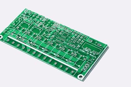
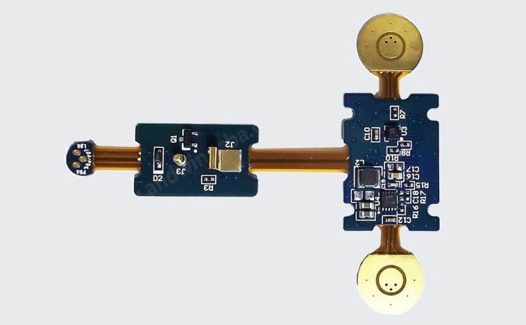
Multi layer flex pcb
Advantages Of Multi-Layer Flex PCB In Modern Electronics
In the rapidly evolving landscape of modern electronics, the demand for more compact, efficient, and reliable components has never been greater. Among the innovations meeting these demands is the multi-layer flexible printed circuit board (PCB), a technology that has revolutionized the way electronic devices are designed and manufactured. Multi-layer flex PCBs offer a myriad of advantages that make them indispensable in contemporary electronic applications, ranging from consumer electronics to aerospace and medical devices.
To begin with, one of the most significant advantages of multi-layer flex PCBs is their ability to save space and reduce weight.
Traditional rigid PCBs can be bulky and limit the design possibilities of electronic devices. In contrast, multi-layer flex PCBs are designed to bend and fold, allowing them to fit into tight spaces and conform to the contours of the device. This flexibility enables designers to create more compact and lightweight products without compromising on functionality. As a result, devices such as smartphones, tablets, and wearable technology have become increasingly slim and portable, meeting consumer demand for convenience and ease of use.
Moreover, multi-layer flex PCBs enhance the reliability and durability of electronic devices.
The flexible nature of these PCBs allows them to absorb shocks and vibrations, which are common in portable and mobile applications. This resilience reduces the risk of damage and extends the lifespan of the device. Additionally, the use of multiple layers in these PCBs facilitates the integration of complex circuits, which can improve the overall performance and functionality of the device. By incorporating multiple layers, designers can achieve higher circuit density, allowing for more sophisticated electronic designs that can handle increased power and data processing requirements.
Another notable advantage of multi-layer flex PCBs is their ability to improve thermal management within electronic devices.
As electronic components become more powerful, they generate more heat, which can affect performance and reliability. Multi-layer flex PCBs can be designed with specific materials and structures that enhance heat dissipation, ensuring that devices operate within safe temperature ranges. This capability is particularly important in high-performance applications such as computing and telecommunications, where efficient thermal management is crucial for maintaining optimal performance.
Furthermore, the versatility of multi-layer flex PCBs makes them suitable for a wide range of applications.
They can be used in environments where traditional PCBs would fail, such as in high-temperature or high-vibration settings. This adaptability opens up new possibilities for innovation in industries such as automotive, aerospace, and medical technology, where reliability and performance are paramount. For instance, in the automotive industry, multi-layer flex PCBs are used in advanced driver-assistance systems (ADAS) and infotainment systems, contributing to the development of smarter and safer vehicles.
In conclusion, the advantages of multi-layer flex PCBs in modern electronics are manifold. Their ability to save space, reduce weight, enhance reliability, improve thermal management, and offer versatility makes them a critical component in the design and manufacture of cutting-edge electronic devices. As technology continues to advance, the role of multi-layer flex PCBs is likely to expand, driving further innovation and enabling the development of even more sophisticated and efficient electronic products.
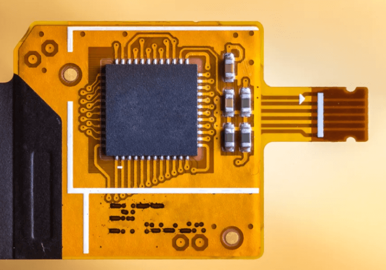
Design Considerations For Multi-Layer Flex PCB
When designing multi-layer flexible printed circuit boards (PCBs), several critical considerations must be taken into account to ensure optimal performance and reliability. Multi-layer flex PCBs are increasingly popular in various industries due to their ability to accommodate complex electronic designs while offering flexibility and space-saving advantages. However, the design process for these intricate circuits requires careful planning and attention to detail.
To begin with, understanding the material properties is essential.
The choice of substrate material significantly impacts the performance of the multi-layer flex PCB. Polyimide is commonly used due to its excellent thermal stability, flexibility, and dielectric properties. However, designers must also consider the adhesive materials used to bond the layers, as these can affect the board’s flexibility and thermal performance. Selecting materials that can withstand the intended operating environment, including temperature fluctuations and mechanical stress, is crucial.
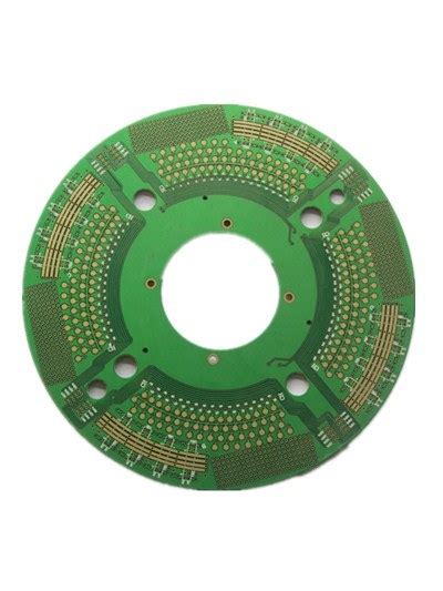
Another important consideration is the layer stack-up configuration.
The number of layers and their arrangement must be carefully planned to balance electrical performance with mechanical flexibility. Designers must ensure that the stack-up supports the necessary signal integrity while minimizing electromagnetic interference (EMI). This often involves strategically placing ground and power planes to provide effective shielding and return paths for signals. Additionally, the use of impedance-controlled traces is vital to maintain signal integrity, especially in high-speed applications.
Transitioning to the layout design, trace routing requires meticulous attention.
The flexible nature of these PCBs means that traces can be subjected to bending and twisting, which can lead to mechanical stress and potential failure. Therefore, it is advisable to use curved traces instead of sharp angles to distribute stress more evenly. Furthermore, maintaining consistent trace widths and spacing is essential to prevent impedance mismatches and signal degradation. Designers should also consider the use of teardrop pads at via and trace junctions to enhance mechanical strength and reduce stress concentrations.
Thermal management is another critical aspect of multi-layer flex PCB design.
The compact nature of these boards can lead to heat accumulation, which can adversely affect performance and reliability. Implementing thermal vias and heat sinks can help dissipate heat effectively. Additionally, selecting materials with high thermal conductivity can aid in managing heat distribution across the board. It is also important to consider the thermal expansion properties of the materials used, as mismatches can lead to delamination or cracking.
Moreover, the mechanical design of the flex PCB must account for the intended application and movement.
Bend radius is a key factor; designing with a larger bend radius can reduce stress on the circuit and enhance durability. It is also advisable to avoid placing components or vias in areas that will experience frequent bending. Reinforcing critical areas with stiffeners can provide additional support and prevent damage.
Finally, manufacturability and cost considerations should not be overlooked.
The complexity of multi-layer flex PCBs can lead to higher production costs, so it is important to work closely with manufacturers to optimize the design for cost-effective production. This includes considering panelization strategies, minimizing the number of layers where possible, and ensuring that the design adheres to standard manufacturing capabilities.
In conclusion, designing multi-layer flex PCBs involves a delicate balance of electrical, mechanical, and thermal considerations. By carefully selecting materials, planning the layer stack-up, optimizing trace routing, managing thermal performance, and considering mechanical constraints, designers can create robust and reliable multi-layer flex PCBs that meet the demands of modern electronic applications.
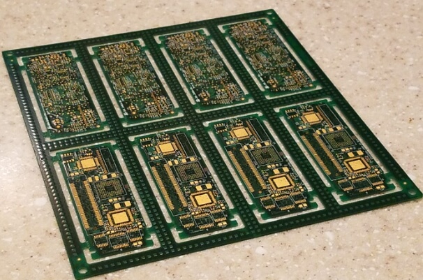
Manufacturing Process Of Multi-Layer Flex PCB
The manufacturing process of multi-layer flex PCBs is a sophisticated and intricate procedure that requires precision and expertise. Multi-layer flex PCBs, known for their flexibility and ability to accommodate complex electronic designs, are increasingly in demand across various industries, including aerospace, medical devices, and consumer electronics. Understanding the manufacturing process of these advanced circuit boards is essential for appreciating their capabilities and applications.
To begin with, the process starts with the design phase, where engineers use specialized software to create a detailed blueprint of the circuit.
This design includes the layout of the conductive paths, the placement of components, and the overall structure of the PCB. Once the design is finalized, it is converted into a format suitable for manufacturing, often using computer-aided design (CAD) tools. This digital representation serves as the foundation for the subsequent steps in the manufacturing process.
Following the design phase, the next step involves selecting the appropriate materials.
Multi-layer flex PCBs are typically made from flexible substrates such as polyimide, which offers excellent thermal stability and flexibility. The choice of materials is crucial, as it directly impacts the performance and durability of the final product. Once the materials are selected, they are prepared for the layering process.
The layering process is a critical stage in the manufacturing of multi-layer flex PCBs.
It involves stacking multiple layers of conductive and insulating materials to form a cohesive unit. Each layer is carefully aligned and bonded together using adhesive materials. This process requires precision to ensure that the layers are correctly aligned, as any misalignment can lead to defects in the final product. Advanced machinery and techniques, such as automated optical inspection, are often employed to maintain accuracy during this stage.
After the layers are bonded, the next step is the drilling process.
This involves creating holes, known as vias, that allow electrical connections between the different layers of the PCB. The drilling process must be executed with high precision to ensure that the vias are correctly positioned and sized. Laser drilling is commonly used for this purpose, as it offers the accuracy and speed required for multi-layer flex PCBs.
Subsequently, the circuit pattern is created through a process called etching.
During etching, unwanted copper is removed from the surface of the PCB, leaving behind the desired circuit pattern. This is achieved by applying a protective mask over the areas that need to remain conductive and then exposing the board to a chemical solution that dissolves the unprotected copper. The result is a precise and intricate circuit pattern that forms the backbone of the PCB’s functionality.
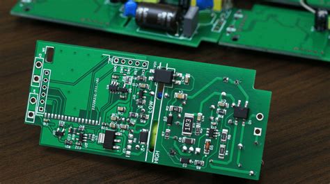
Once the etching process is complete, the PCB undergoes a series of finishing steps.
These include applying a solder mask to protect the circuit from environmental factors and adding surface finishes to enhance solderability. Additionally, electrical testing is conducted to ensure that the PCB functions as intended and meets the required specifications.
In conclusion, the manufacturing process of multi-layer flex PCBs is a complex and meticulous procedure that involves several critical stages, from design and material selection to layering, drilling, etching, and finishing. Each step requires precision and expertise to produce a high-quality product that meets the demands of modern electronic applications. As technology continues to advance, the importance of understanding and mastering this process becomes increasingly significant, paving the way for innovative solutions in various industries.
Applications Of Multi-Layer Flex PCB In Various Industries
Multi-layer flexible printed circuit boards (PCBs) have emerged as a pivotal innovation in the electronics industry, offering a versatile solution that caters to the evolving demands of modern technology. These advanced PCBs are characterized by their ability to bend and flex, which allows them to be integrated into a wide array of applications across various industries. As we delve into the applications of multi-layer flex PCBs, it becomes evident that their unique properties have revolutionized the way electronic devices are designed and utilized.
In the consumer electronics sector, multi-layer flex PCBs have become indispensable due to their ability to accommodate complex circuitry within compact spaces.
Smartphones, tablets, and wearable devices are prime examples where these PCBs are extensively used. The flexibility of the circuit boards allows manufacturers to design sleeker and more ergonomic devices without compromising on functionality. Moreover, the durability and reliability of multi-layer flex PCBs ensure that these devices can withstand the rigors of daily use, including bending and twisting, which are common in portable electronics.
Transitioning to the automotive industry, the integration of multi-layer flex PCBs has significantly enhanced the performance and functionality of modern vehicles.
With the increasing demand for advanced driver-assistance systems (ADAS), infotainment systems, and electric vehicle components, the need for compact and reliable electronic solutions has never been greater. Multi-layer flex PCBs offer the perfect solution by providing the necessary flexibility and robustness required in automotive applications. They are used in various components, including sensors, control units, and lighting systems, contributing to the overall efficiency and safety of vehicles.
In the realm of medical devices, the application of multi-layer flex PCBs has been transformative.
The medical industry requires devices that are not only highly reliable but also capable of accommodating intricate designs. Multi-layer flex PCBs meet these requirements by enabling the development of compact and lightweight medical devices such as pacemakers, hearing aids, and diagnostic equipment. Their flexibility allows for the creation of devices that can conform to the human body, enhancing patient comfort and device efficacy. Furthermore, the ability to integrate multiple layers of circuitry within a single board reduces the overall size of medical devices, making them more portable and user-friendly.
The aerospace and defense industries also benefit significantly from the use of multi-layer flex PCBs.
In these sectors, the demand for lightweight and reliable electronic components is paramount due to the harsh operating environments and stringent performance requirements. Multi-layer flex PCBs are utilized in various applications, including communication systems, navigation equipment, and control systems. Their ability to withstand extreme temperatures and vibrations makes them ideal for use in aircraft and military equipment, where reliability is crucial.
In conclusion, the applications of multi-layer flex PCBs across various industries underscore their importance in modern technology. Their unique properties, including flexibility, durability, and the ability to accommodate complex circuitry, make them an invaluable component in the design and functionality of electronic devices. As technology continues to advance, the role of multi-layer flex PCBs is expected to expand further, driving innovation and efficiency across multiple sectors. The versatility and adaptability of these PCBs ensure that they will remain a cornerstone of electronic design for years to come.