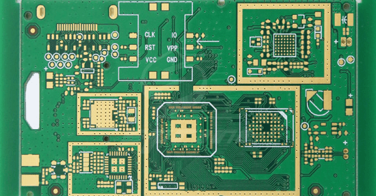
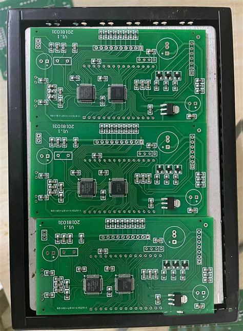
Multi layer flexible pcb
Advantages Of Multi-Layer Flexible PCBs In Modern Electronics
In the rapidly evolving landscape of modern electronics, the demand for more compact, efficient, and versatile components has led to significant advancements in printed circuit board (PCB) technology. Among these innovations, multi-layer flexible PCBs have emerged as a pivotal solution, offering a range of advantages that cater to the needs of contemporary electronic devices. As we delve into the benefits of multi-layer flexible PCBs, it becomes evident that their unique properties are instrumental in shaping the future of electronic design and manufacturing.
To begin with, one of the most notable advantages of multi-layer flexible PCBs is their ability to accommodate complex circuit designs within a compact form factor.
Unlike traditional rigid PCBs, which are limited by their inflexible nature, multi-layer flexible PCBs can be bent, folded, and twisted to fit into tight spaces. This flexibility is particularly beneficial in applications where space is at a premium, such as in wearable technology, medical devices, and compact consumer electronics. By enabling more intricate designs, these PCBs allow engineers to maximize functionality without compromising on size or weight.
Moreover, the inherent flexibility of these PCBs contributes to enhanced durability and reliability.
In environments where electronic devices are subject to constant movement or vibration, such as in automotive or aerospace applications, the ability of multi-layer flexible PCBs to withstand mechanical stress without breaking is invaluable. This resilience not only extends the lifespan of the devices but also reduces the likelihood of failure, thereby ensuring consistent performance over time. Consequently, manufacturers can achieve higher levels of quality assurance, which is crucial in industries where reliability is paramount.
In addition to their physical adaptability, multi-layer flexible PCBs offer significant electrical advantages.
The use of multiple layers allows for more efficient routing of electrical signals, reducing the need for long, convoluted pathways that can introduce signal interference and loss. This results in improved signal integrity and faster data transmission, which are critical factors in high-speed electronic applications. Furthermore, the ability to integrate multiple functions within a single PCB reduces the need for additional components, leading to cost savings in both materials and assembly.
Another compelling benefit of multi-layer flexible PCBs is their contribution to environmental sustainability.
As the electronics industry faces increasing pressure to minimize its ecological footprint, the use of flexible PCBs can play a role in reducing waste. Their lightweight nature means that less material is required for production, and their durability ensures a longer product lifecycle, both of which contribute to a reduction in electronic waste. Additionally, advancements in manufacturing processes have made it possible to produce these PCBs with environmentally friendly materials, further aligning with global sustainability goals.
In conclusion, the advantages of multi-layer flexible PCBs in modern electronics are manifold, encompassing design flexibility, durability, electrical performance, and environmental sustainability. As technology continues to advance, the role of these innovative PCBs is likely to expand, driving further improvements in electronic device design and functionality. By embracing the potential of multi-layer flexible PCBs, manufacturers can not only meet the demands of today’s market but also pave the way for future innovations that will continue to transform the electronics industry.
Design Considerations For Multi-Layer Flexible PCBs
When designing multi-layer flexible printed circuit boards (PCBs), several critical considerations must be taken into account to ensure optimal performance and reliability. These advanced circuit boards, which offer the benefits of flexibility and compactness, are increasingly used in a variety of applications, from consumer electronics to aerospace systems. As such, understanding the nuances of their design is essential for engineers and designers aiming to leverage their full potential.
To begin with, material selection is a fundamental aspect of designing multi-layer flexible PCBs.
The choice of substrate material significantly influences the board’s flexibility, thermal stability, and overall durability. Polyimide is a popular choice due to its excellent thermal resistance and mechanical properties. However, the specific application requirements may necessitate the use of other materials, such as polyester or liquid crystal polymer, each offering distinct advantages and limitations. Therefore, a thorough evaluation of the material properties in relation to the intended application is crucial.
In addition to material selection, the stack-up configuration of the layers is another vital consideration.
The stack-up determines the electrical performance, impedance control, and mechanical flexibility of the PCB. Designers must carefully plan the arrangement of signal, power, and ground layers to minimize electromagnetic interference and ensure signal integrity. Moreover, the use of adhesive layers between the flexible substrates should be optimized to maintain flexibility while providing adequate bonding strength. This balance is essential to prevent delamination and ensure the longevity of the PCB in dynamic environments.
Furthermore, trace routing and layout design play a significant role in the functionality of multi-layer flexible PCBs.
The routing of traces must be meticulously planned to avoid sharp bends and excessive stress, which can lead to trace cracking or failure. Employing curved traces and maintaining a consistent bend radius can help mitigate these risks. Additionally, the layout should consider the distribution of components and vias to minimize stress concentration and enhance the board’s mechanical resilience. By strategically placing components and optimizing the via structure, designers can improve the board’s reliability and performance.
Thermal management is another critical aspect that cannot be overlooked in the design of multi-layer flexible PCBs.
The compact nature of these boards often results in higher power densities, necessitating effective heat dissipation strategies. Incorporating thermal vias, heat sinks, or conductive layers can help manage heat distribution and prevent overheating. Moreover, understanding the thermal expansion properties of the materials used is essential to avoid mechanical stress and potential failure due to temperature fluctuations.
Finally, manufacturability and cost considerations are integral to the design process.
While multi-layer flexible PCBs offer numerous advantages, their complexity can lead to higher manufacturing costs. Designers must work closely with manufacturers to ensure that the design is feasible and cost-effective. This collaboration can involve selecting appropriate manufacturing techniques, such as roll-to-roll processing or laser cutting, to optimize production efficiency and reduce costs.
In conclusion, designing multi-layer flexible PCBs requires a comprehensive understanding of various factors, including material selection, stack-up configuration, trace routing, thermal management, and manufacturability. By carefully considering these elements, designers can create robust and reliable PCBs that meet the demands of modern applications. As technology continues to advance, the importance of these considerations will only grow, underscoring the need for meticulous design practices in the development of flexible electronic solutions.
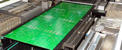
Manufacturing Process Of Multi-Layer Flexible PCBs
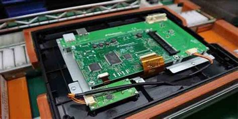
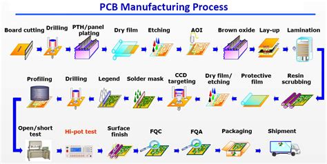
The manufacturing process of multi-layer flexible printed circuit boards (PCBs) is a sophisticated and intricate procedure that requires precision and expertise. These advanced PCBs are essential in modern electronics, offering flexibility, reduced weight, and the ability to fit into compact spaces, making them ideal for a wide range of applications, from consumer electronics to aerospace technology. Understanding the manufacturing process of these multi-layer flexible PCBs is crucial for appreciating their complexity and the technological advancements they represent.
To begin with, the process starts with the selection of appropriate materials.
The base material typically used is a flexible substrate, such as polyimide, which provides the necessary flexibility and thermal stability. This substrate is coated with a thin layer of copper, which serves as the conductive material. The choice of materials is critical, as it influences the performance, durability, and flexibility of the final product.
Following the material selection, the next step involves the design and layout of the circuit.
Advanced computer-aided design (CAD) software is employed to create precise and intricate circuit patterns. This design phase is crucial, as it determines the functionality and efficiency of the PCB. Once the design is finalized, it is transferred onto the flexible substrate through a process known as photolithography. This involves coating the substrate with a photosensitive material, exposing it to ultraviolet light through a mask that contains the circuit pattern, and then developing the image to reveal the desired circuit layout.
Subsequently, the etching process takes place, where unwanted copper is removed to leave behind the circuit pattern.
This is achieved through chemical etching, where the substrate is immersed in an etching solution that dissolves the exposed copper. The precision of this step is vital, as any errors can lead to circuit failures or inefficiencies.
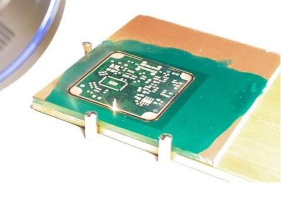
Once the etching is complete, the next phase involves the lamination of multiple layers.
This is where the multi-layer aspect of the PCB comes into play. Each layer is carefully aligned and bonded together using adhesive materials and heat. The lamination process requires meticulous attention to detail to ensure that the layers are perfectly aligned and that there are no air bubbles or misalignments, which could compromise the integrity of the PCB.
After lamination, the vias, or interlayer connections, are created.
This involves drilling tiny holes through the layers and plating them with copper to establish electrical connections between different layers. The precision of this step is paramount, as it ensures the seamless flow of electrical signals throughout the PCB.
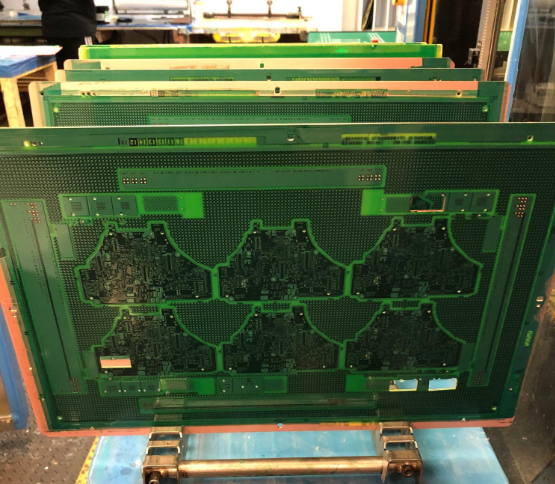
Finally, the PCB undergoes a series of tests and inspections to verify its functionality and reliability. These tests include electrical testing to check for continuity and isolation, as well as visual inspections to identify any physical defects. Once the PCB passes these rigorous tests, it is ready for integration into electronic devices.
In conclusion, the manufacturing process of multi-layer flexible PCBs is a complex and meticulous procedure that combines advanced materials, precise design, and sophisticated techniques. Each step, from material selection to final testing, plays a crucial role in ensuring the performance and reliability of these essential components in modern electronics. As technology continues to evolve, the demand for these versatile and efficient PCBs is expected to grow, further highlighting the importance of understanding their manufacturing process.
Applications Of Multi-Layer Flexible PCBs In Various Industries
Multi-layer flexible printed circuit boards (PCBs) have emerged as a pivotal technology in the electronics industry, offering a unique combination of flexibility, durability, and compactness. These attributes make them indispensable in a wide array of applications across various industries. As technology continues to advance, the demand for more sophisticated electronic devices has led to the increased adoption of multi-layer flexible PCBs, which are now integral to the design and functionality of many modern devices.
In the consumer electronics sector, multi-layer flexible PCBs are extensively used in smartphones, tablets, and wearable devices.
The compact and lightweight nature of these PCBs allows manufacturers to design sleeker and more portable devices without compromising on performance. Moreover, the flexibility of these PCBs enables the integration of complex circuits in limited spaces, which is crucial for the development of advanced features in consumer electronics. As a result, multi-layer flexible PCBs contribute significantly to the miniaturization trend in this industry, allowing for the creation of devices that are not only more efficient but also more aesthetically appealing.
Transitioning to the automotive industry, multi-layer flexible PCBs play a critical role in the development of modern vehicles.
With the increasing incorporation of electronic systems in cars, such as advanced driver-assistance systems (ADAS), infotainment systems, and electric vehicle components, the need for reliable and flexible circuit solutions has become paramount. Multi-layer flexible PCBs offer the necessary durability and adaptability to withstand the harsh conditions within automotive environments, including extreme temperatures and vibrations. Consequently, they are essential in ensuring the seamless operation of various electronic systems, thereby enhancing vehicle safety, performance, and user experience.
In the realm of medical devices, the application of multi-layer flexible PCBs is equally transformative.
Medical technology demands high precision and reliability, and these PCBs provide the necessary attributes to meet such stringent requirements. They are used in a variety of medical devices, including diagnostic equipment, wearable health monitors, and implantable devices. The flexibility and biocompatibility of these PCBs allow for the development of devices that can conform to the human body, providing more accurate readings and improving patient comfort. Furthermore, the ability to incorporate multiple layers of circuitry in a compact form factor is crucial for the development of sophisticated medical devices that can perform complex functions while remaining minimally invasive.
In addition to these industries, multi-layer flexible PCBs are also making significant inroads into the aerospace and defense sectors.
The demanding conditions of aerospace applications require components that are not only lightweight but also capable of withstanding extreme environmental stresses. Multi-layer flexible PCBs meet these criteria, offering high reliability and performance in critical applications such as satellite systems, avionics, and military communication devices. Their ability to maintain functionality under extreme conditions makes them an ideal choice for aerospace and defense applications, where failure is not an option.
In conclusion, the versatility and advanced capabilities of multi-layer flexible PCBs have made them a cornerstone technology across various industries. As the demand for more compact, efficient, and reliable electronic solutions continues to grow, the role of these PCBs is set to expand even further. By enabling the development of cutting-edge devices and systems, multi-layer flexible PCBs are not only shaping the present landscape of technology but also paving the way for future innovations.