Multi Printed Circuit Boards Ltd: Cutting-Edge PCB Manufacturing
Key Takeaways
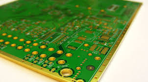
When exploring PCB manufacturing options, you need to prioritize three core elements: technical expertise, cost efficiency, and industry-specific adaptability. Leading PCB manufacturing companies distinguish themselves by integrating advanced fabrication processes with rigorous quality controls, ensuring reliability for high-stakes sectors like aerospace and IoT.
A critical consideration is PCB manufacturing cost, which hinges on factors like material selection, layer complexity, and production volume. For example:
| Cost Factor | Impact Level | Optimization Strategy |
|---|---|---|
| Material Grade | High | Balance durability and budget |
| Layer Count | Moderate | Simplify designs where possible |
| Order Volume | High | Leverage bulk pricing discounts |
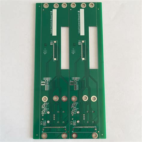
In the PCB manufacturing business, customization is key. Whether you require ultra-thin boards for wearable tech or high-frequency substrates for telecom infrastructure, suppliers must offer tailored design strategies to meet evolving industry demands. Companies that excel in PCB manufacturing often provide end-to-end solutions—from prototyping to mass production—while maintaining compliance with industry-standard PCB production guidelines.
By aligning your project’s requirements with a manufacturer’s technical capabilities and cost structures, you can optimize both performance and budget. This approach ensures seamless integration of cutting-edge PCBs into your products, regardless of sector-specific challenges.
Advanced PCB Manufacturing Techniques
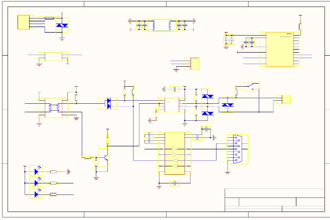
When exploring PCB manufacturing advancements, you’ll find modern techniques prioritize precision, scalability, and material innovation. Leading PCB manufacturing companies now employ automated optical inspection (AOI) systems to detect micron-level defects, ensuring flawless boards even in high-volume production. Laser direct imaging (LDI) further enhances accuracy by eliminating photomasks, reducing errors in complex designs—critical for industries like aerospace where tolerances are razor-thin.
"Optimizing PCB manufacturing cost requires balancing advanced technologies with material efficiency. Consider hybrid stack-ups combining high-frequency laminates and standard FR-4 to meet performance goals without overspending."
For your PCB manufacturing business, adopting additive processes like semi-additive fabrication (mSAP) can minimize copper waste while enabling ultra-fine circuitry. Embedded component technology also reduces assembly steps, cutting both time and expenses. When selecting partners, prioritize those offering design for manufacturability (DFM) analysis—this preemptively addresses layout flaws that could escalate costs or delay timelines.
From rigid-flex boards for wearable IoT devices to heavy-copper PCBs for power systems, these techniques ensure your projects stay competitive. By leveraging cutting-edge methods, you achieve not just technical excellence but also scalability across diverse applications.
Aerospace-Grade Circuit Board Tech
When designing electronics for aerospace applications, you need PCB manufacturing solutions that meet extreme performance thresholds. Aerospace-grade circuit boards must withstand thermal cycling, high-frequency vibrations, and radiation exposure while maintaining signal integrity across mission-critical systems. Leading PCB manufacturing companies leverage specialized materials like polyimide substrates and ceramic-filled laminates to ensure reliability in low-pressure environments or rapid temperature shifts.
Balancing PCB manufacturing cost with uncompromising quality is key here. While aerospace projects often prioritize durability over budget constraints, advanced fabrication techniques—such as laser-drilled microvias and embedded component technology—help reduce material waste and assembly complexity. These innovations enable tighter integration of circuitry without sacrificing compliance with MIL-PRF-31032 or AS9100 standards.
For businesses in this sector, optimizing the PCB manufacturing business model means investing in precision etching equipment and rigorous testing protocols. Automated optical inspection (AOI) and X-ray analysis are critical for detecting micron-level defects in multilayer boards. By aligning design strategies with aerospace requirements, manufacturers can deliver boards that excel in avionics, satellite communications, and navigation systems—laying the groundwork for seamless transitions into telecom and IoT applications later in the production chain.
Telecom Sector PCB Innovations
The telecom industry’s relentless demand for faster data transfer and enhanced connectivity drives continuous advancements in PCB manufacturing. As 5G networks expand globally, PCB manufacturing companies must prioritize designs that minimize signal loss while maximizing bandwidth efficiency. High-frequency materials like Rogers substrates and low-loss laminates are now standard for telecom-grade boards, ensuring stable performance in millimeter-wave applications.
Balancing PCB manufacturing cost with performance remains critical, especially for large-scale infrastructure projects. Leading providers optimize layer stacking and integrate embedded components to reduce material waste and assembly steps. This approach not only lowers expenses but also aligns with the telecom sector’s need for compact, high-density interconnects.
For businesses navigating this competitive landscape, partnering with a PCB manufacturing business that specializes in high-speed digital (HSD) and radio frequency (RF) designs can be transformative. Innovations like hybrid rigid-flex boards enable seamless integration into base stations and small-cell deployments, addressing both durability and space constraints.
By leveraging cutting-edge fabrication techniques—such as laser-drilled microvias and automated optical inspection (AOI)—manufacturers ensure compliance with stringent industry standards. These advancements underscore how strategic PCB manufacturing partnerships empower telecom operators to stay ahead in an era defined by hyperconnectivity and evolving network architectures.
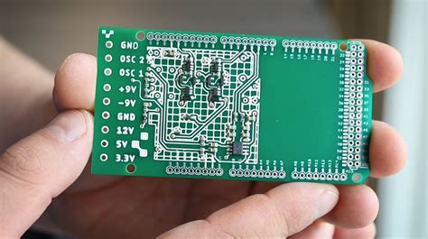
IoT Device PCB Customization
When developing IoT devices, you need PCB manufacturing solutions that balance compact design with robust functionality. Miniaturization remains critical, as space-constrained sensors and wearables demand ultra-thin, high-density boards. Leading PCB manufacturing companies leverage HDI (High-Density Interconnect) technology to embed microvias and fine traces, ensuring signal integrity even in palm-sized devices.
Cost efficiency becomes paramount at scale, which is why optimizing PCB manufacturing cost requires strategic material selection. For example, using flexible substrates reduces assembly steps while accommodating irregular form factors—common in smart home gadgets. Thermal management also takes center stage, with advanced heat-dissipating materials preventing performance drops in always-on IoT systems.
For businesses scaling production, partnering with a PCB manufacturing business that specializes in IoT ensures seamless integration of wireless modules (like Bluetooth or LoRaWAN) and power-efficient layouts. Prototyping phases often benefit from rapid-turn services, allowing you to test antenna placement and power consumption before mass production. By aligning design choices with manufacturing capabilities early, you avoid costly revisions and accelerate time-to-market for connected devices.
Precision Engineering in PCB Production
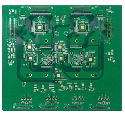
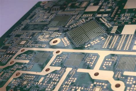
Achieving micrometer-level accuracy in PCB manufacturing requires meticulous attention to material selection, process control, and advanced equipment. Modern precision engineering ensures that even the most complex multi-layer designs meet exacting standards for signal integrity and thermal management. Leading PCB manufacturing companies leverage laser drilling and automated optical inspection (AOI) systems to eliminate defects, reducing PCB manufacturing cost through minimized material waste and rework.
For industries like aerospace or medical devices, where reliability is non-negotiable, these precision techniques translate to boards capable of withstanding extreme temperatures and vibrations. Advanced etching technologies enable finer trace widths, while impedance-controlled routing maintains signal clarity in high-frequency applications. When evaluating PCB manufacturing business partnerships, prioritize providers with ISO-certified workflows and real-time quality monitoring—critical for balancing performance demands with budget constraints.
By integrating AI-driven design validation and closed-loop feedback systems, manufacturers ensure every board aligns with your specifications before production begins. This approach not only accelerates time-to-market but also future-proofs your electronics against evolving industry requirements.
Cutting-Edge PCB Tech Applications
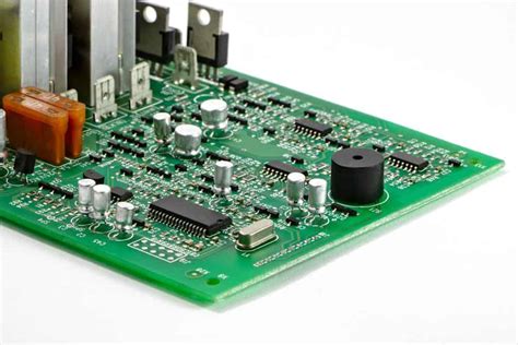
When exploring modern PCB manufacturing solutions, you’ll find that today’s pcb manufacturing companies leverage technologies designed to optimize performance while managing pcb manufacturing cost. For instance, high-density interconnect (HDI) boards enable miniaturization in wearable devices, while flexible PCBs support dynamic form factors for aerospace instrumentation. These advancements are critical for industries requiring precision, durability, and adaptability—from medical implants to 5G infrastructure.
Thermal management innovations, such as embedded copper substrates, address heat dissipation challenges in high-power telecom systems, directly impacting long-term reliability. Meanwhile, additive manufacturing techniques reduce material waste, aligning with sustainability goals without compromising pcb manufacturing business scalability. By integrating AI-driven quality control, manufacturers ensure defect rates stay below 0.1%, even in complex multilayer designs.
For IoT applications, pcb manufacturing now incorporates edge-plated connectors and ultra-low-loss laminates to maintain signal integrity across smart sensors. This approach balances pcb manufacturing cost with performance demands, allowing businesses to deploy scalable solutions across global networks. Whether prototyping or mass production, these technologies ensure your projects stay ahead in a rapidly evolving electronics landscape.
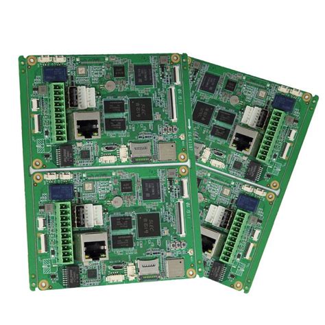
Expert PCB Solutions for Industries
When selecting PCB manufacturing companies for industrial applications, you need partners who understand the unique demands of your sector. Leading providers combine precision engineering with scalable production to deliver solutions that balance PCB manufacturing cost with performance requirements. Whether you’re developing mission-critical aerospace systems or high-volume IoT devices, tailored approaches ensure compliance with industry-specific standards like MIL-PRF-31032 or ISO 13485.
Advanced PCB manufacturing workflows now integrate AI-driven design validation and automated testing, minimizing errors while accelerating time-to-market. For industries like telecom, where signal integrity is non-negotiable, multilayer boards with impedance control become essential. Meanwhile, IoT developers benefit from flexible low-power designs that optimize energy efficiency without compromising functionality.
A successful PCB manufacturing business thrives on adaptability. Look for suppliers offering rapid prototyping and material diversification—from high-frequency Rogers substrates to flame-retardant FR-4 variants. Transparent cost structures and DFM (Design for Manufacturing) analysis further ensure your projects stay within budget while meeting rigorous quality benchmarks. By aligning technical expertise with your operational goals, you gain reliability in every circuit—no matter how complex the application.
Custom Circuit Board Design Strategies
When developing custom circuit boards, aligning your design with PCB manufacturing capabilities ensures optimal performance and reliability. Leading PCB manufacturing companies emphasize early collaboration to address technical constraints, such as layer stack-up configurations or impedance control requirements. By leveraging advanced design-for-manufacturability (DFM) tools, you can minimize PCB manufacturing cost while maintaining precision—critical for industries like aerospace or IoT, where component density and thermal management are non-negotiable.
A strategic focus on material selection—such as high-frequency laminates for telecom applications or flexible substrates for wearables—directly impacts both functionality and scalability in the PCB manufacturing business. Tools like automated routing and simulation software help validate designs before prototyping, reducing iteration cycles. Iterative testing and adherence to industry standards (IPC-6012, for example) further ensure compliance with rigorous operational environments. This approach not only streamlines production but also future-proofs your electronics against evolving technological demands.
Conclusion
When navigating the complexities of PCB manufacturing, your choice of partner ultimately determines the success of your electronic projects. Leading PCB manufacturing companies like Multi Printed Circuit Boards Ltd demonstrate how integrating advanced technologies with precision engineering can address diverse industry demands—from aerospace to IoT. As you evaluate options, consider how innovative design strategies and material optimization directly influence PCB manufacturing cost, ensuring you balance budget constraints with performance requirements.
For businesses scaling their PCB manufacturing business, prioritizing adaptability and quality control remains non-negotiable. Whether you’re prototyping or moving to mass production, aligning with experts who specialize in custom solutions ensures your designs meet rigorous standards. By focusing on end-use applications—such as high-frequency telecom systems or compact IoT devices—you gain access to tailored workflows that minimize waste and accelerate time-to-market.
In an era where electronics evolve rapidly, partnering with forward-thinking manufacturers empowers you to stay competitive. The right collaboration transforms technical challenges into opportunities, reinforcing why strategic decisions in PCB manufacturing shape the future of your industry.
Frequently Asked Questions
What should you look for in reliable PCB manufacturing companies?
When selecting partners for PCB manufacturing, prioritize firms with ISO-certified facilities and proven expertise in your industry. Leading providers combine automated production lines with rigorous testing protocols to ensure precision and reliability across batches.
How does PCB manufacturing cost vary across projects?
Costs depend on design complexity, material choices (like high-frequency laminates), and order volumes. Prototyping typically incurs higher per-unit expenses, while bulk orders benefit from economies of scale. Transparent PCB manufacturing business models provide detailed breakdowns during quoting.
Can customized PCBs meet aerospace or medical compliance standards?
Yes, specialized PCB manufacturing services implement MIL-spec protocols, impedance control, and HDI layouts to satisfy industry-specific certifications. Providers with defense or healthcare sector experience optimize designs for extreme temperatures and signal integrity.
What innovations are shaping modern PCB manufacturing?
Advancements like embedded components, flexible substrates, and additive manufacturing enable lighter, denser boards. Forward-looking PCB manufacturing companies now integrate AI-driven quality checks and IoT-enabled supply chain tracking to reduce lead times.
Ready to Optimize Your Electronics Project?
For tailored solutions that balance PCB manufacturing cost with performance demands, please click here to consult engineers specializing in mission-critical applications.