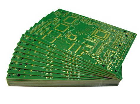
Multilayer pcb 3d
Advantages Of Multilayer PCB 3D Design In Modern Electronics
In the rapidly evolving landscape of modern electronics, the demand for more compact, efficient, and powerful devices has led to significant advancements in printed circuit board (PCB) technology. Among these advancements, multilayer PCB 3D design stands out as a pivotal innovation, offering numerous advantages that cater to the needs of contemporary electronic applications. As electronic devices become increasingly complex, the integration of multilayer PCB 3D design has become essential in meeting the stringent requirements of modern technology.
One of the primary advantages of multilayer PCB 3D design is its ability to significantly reduce the size and weight of electronic devices.
By stacking multiple layers of circuitry within a single board, designers can achieve a higher density of components without expanding the physical footprint of the device. This compactness is particularly beneficial in applications where space is at a premium, such as in smartphones, wearable technology, and medical devices. The reduction in size not only enhances portability but also contributes to the aesthetic appeal of consumer electronics, which is a crucial factor in today’s competitive market.
Moreover, multilayer PCB 3D design enhances the performance and reliability of electronic devices.
The close proximity of the layers allows for shorter interconnections, which in turn reduces signal loss and improves the overall speed of data transmission. This is especially important in high-frequency applications where signal integrity is paramount. Additionally, the use of multiple layers facilitates better power distribution and ground planes, which help in minimizing electromagnetic interference (EMI) and ensuring stable operation. As a result, devices equipped with multilayer PCBs exhibit superior performance and are less prone to malfunctions, thereby increasing their longevity and user satisfaction.
Furthermore, the flexibility offered by multilayer PCB 3D design enables more sophisticated and intricate circuit designs.
Engineers can implement complex routing schemes and integrate a multitude of components, such as microprocessors, memory modules, and sensors, within a single board. This capability is crucial in the development of advanced technologies like artificial intelligence, the Internet of Things (IoT), and autonomous systems, where intricate circuitry is required to process vast amounts of data efficiently. The ability to accommodate such complexity within a compact form factor is a testament to the versatility of multilayer PCB 3D design.
In addition to these technical benefits, multilayer PCB 3D design also contributes to cost-effectiveness in the manufacturing process.
Although the initial design and fabrication of multilayer PCBs may involve higher costs compared to single-layer boards, the long-term benefits often outweigh these expenses. The reduction in material usage, coupled with the potential for automated assembly processes, can lead to significant cost savings in mass production. Moreover, the enhanced reliability and performance of multilayer PCBs can reduce the need for frequent repairs and replacements, further contributing to cost efficiency over the product’s lifecycle.
In conclusion, the advantages of multilayer PCB 3D design in modern electronics are manifold, encompassing size reduction, performance enhancement, design flexibility, and cost-effectiveness. As the demand for more advanced and compact electronic devices continues to grow, the adoption of multilayer PCB 3D design is poised to play a crucial role in shaping the future of technology. By leveraging these benefits, manufacturers can develop cutting-edge products that meet the ever-evolving needs of consumers and industries alike, thereby driving innovation and progress in the field of electronics.
Innovations In Multilayer PCB 3D Printing Technology
The realm of electronics manufacturing has witnessed a significant transformation with the advent of multilayer PCB 3D printing technology. This innovative approach has revolutionized the way printed circuit boards (PCBs) are designed and produced, offering unprecedented flexibility and efficiency. As the demand for more compact and complex electronic devices continues to grow, the need for advanced PCB solutions becomes increasingly critical. Multilayer PCB 3D printing technology addresses this demand by enabling the creation of intricate, multi-layered circuit boards with remarkable precision and speed.
Traditionally, the production of multilayer PCBs involved a complex and time-consuming process that required multiple steps, including etching, drilling, and lamination.
This conventional method often resulted in longer lead times and higher production costs. However, with the introduction of 3D printing technology, these challenges are being effectively mitigated. By utilizing additive manufacturing techniques, multilayer PCB 3D printing allows for the simultaneous deposition of conductive and insulating materials, thereby streamlining the fabrication process. This not only reduces the time required to produce PCBs but also minimizes material waste, making it a more sustainable option.
Moreover, the versatility of multilayer PCB 3D printing technology is one of its most compelling advantages.
It enables the creation of complex geometries and intricate designs that were previously difficult or impossible to achieve with traditional methods. This capability is particularly beneficial for industries such as aerospace, automotive, and consumer electronics, where space constraints and performance requirements necessitate highly customized solutions. By leveraging 3D printing, engineers can design PCBs with unique shapes and configurations, optimizing the use of available space and enhancing the overall functionality of electronic devices.
In addition to its design flexibility, multilayer PCB 3D printing technology also offers significant improvements in terms of prototyping and testing.
The rapid prototyping capabilities of 3D printing allow engineers to quickly iterate and refine their designs, accelerating the development process. This is especially advantageous in fast-paced industries where time-to-market is a critical factor. Furthermore, the ability to produce functional prototypes in-house reduces the reliance on external suppliers, providing companies with greater control over their production timelines and costs.
As the technology continues to evolve, ongoing research and development efforts are focused on enhancing the performance and reliability of 3D-printed multilayer PCBs.
Innovations in materials science are playing a crucial role in this regard, with the development of advanced conductive inks and dielectric materials that offer improved electrical and thermal properties. These advancements are paving the way for the production of high-performance PCBs that can withstand the demanding conditions of modern electronic applications.
Despite the numerous advantages, it is important to acknowledge the challenges that remain in the widespread adoption of multilayer PCB 3D printing technology.
Issues such as the scalability of production processes, the resolution of printed features, and the integration of different materials are areas that require further exploration and refinement. Nevertheless, the potential benefits of this technology are undeniable, and its continued development is likely to have a profound impact on the electronics manufacturing industry.
In conclusion, multilayer PCB 3D printing technology represents a significant leap forward in the design and production of printed circuit boards. By offering enhanced design flexibility, rapid prototyping capabilities, and improved sustainability, it addresses many of the limitations associated with traditional manufacturing methods. As research and development efforts continue to advance this technology, it is poised to play an increasingly important role in shaping the future of electronics manufacturing, driving innovation and efficiency across a wide range of industries.
Challenges And Solutions In Multilayer PCB 3D Manufacturing
The manufacturing of multilayer printed circuit boards (PCBs) in three dimensions presents a unique set of challenges and opportunities that are reshaping the landscape of electronic design and production. As the demand for more compact, efficient, and powerful electronic devices continues to grow, the industry is increasingly turning to multilayer PCB 3D manufacturing as a solution. However, this innovative approach is not without its hurdles, which require careful consideration and strategic solutions.
One of the primary challenges in multilayer PCB 3D manufacturing is the complexity of design.
Unlike traditional two-dimensional PCBs, 3D multilayer boards require intricate planning to ensure that all layers are correctly aligned and interconnected. This complexity is compounded by the need to accommodate various components and pathways within a limited space. To address this, advanced computer-aided design (CAD) software is employed, allowing engineers to visualize and simulate the entire structure before production begins. This not only helps in identifying potential design flaws but also optimizes the layout for better performance and reliability.
In addition to design complexity, the manufacturing process itself poses significant challenges.
The precision required in layering and aligning multiple PCB layers is critical, as even minor misalignments can lead to functional failures. To mitigate this risk, manufacturers are increasingly utilizing automated processes and high-precision machinery. These technologies ensure that each layer is accurately placed and bonded, reducing the likelihood of errors and improving overall yield.
Another challenge is the thermal management of multilayer PCB 3D structures.
As electronic devices become more powerful, they generate more heat, which can adversely affect performance and longevity. In a 3D multilayer configuration, heat dissipation becomes even more critical due to the compact nature of the design. Innovative solutions such as the integration of thermal vias, heat sinks, and advanced materials with superior thermal conductivity are being employed to address this issue. These solutions help in efficiently managing heat, thereby enhancing the reliability and performance of the final product.
Furthermore, the inspection and testing of multilayer PCB 3D assemblies present their own set of challenges.
Traditional inspection methods may not be sufficient to detect defects in such complex structures. Consequently, manufacturers are adopting advanced testing techniques, including X-ray inspection and automated optical inspection (AOI), to ensure the integrity of the boards. These methods allow for a thorough examination of each layer and interconnection, ensuring that any defects are identified and rectified before the product reaches the market.
Despite these challenges, the benefits of multilayer PCB 3D manufacturing are substantial.
The ability to pack more functionality into a smaller space is a significant advantage, particularly in industries such as consumer electronics, aerospace, and medical devices, where size and weight are critical factors. Moreover, the enhanced performance and reliability offered by these advanced PCBs make them an attractive option for high-performance applications.
In conclusion, while the challenges associated with multilayer PCB 3D manufacturing are considerable, they are not insurmountable. Through the use of advanced design tools, precision manufacturing techniques, effective thermal management solutions, and rigorous testing protocols, the industry is well-equipped to overcome these obstacles. As technology continues to evolve, it is likely that multilayer PCB 3D manufacturing will play an increasingly important role in the development of next-generation electronic devices, offering new possibilities for innovation and efficiency.
Future Trends In Multilayer PCB 3D Applications
The evolution of multilayer printed circuit boards (PCBs) has been a cornerstone in the advancement of modern electronics, and the integration of three-dimensional (3D) technology into these systems is poised to revolutionize the industry further. As we look to the future, the convergence of multilayer PCB technology with 3D applications presents a myriad of opportunities and challenges that are set to redefine the landscape of electronic design and manufacturing.
To begin with, the primary advantage of integrating 3D technology into multilayer PCBs is the potential for increased functionality within a smaller footprint.
Traditional PCBs are limited by their planar nature, which restricts the amount of circuitry that can be accommodated within a given area. However, by leveraging 3D technology, designers can create more complex and compact designs that incorporate multiple layers of circuitry in a three-dimensional space. This not only allows for more components to be included in a single board but also enhances the overall performance and efficiency of the device.
Moreover, the use of 3D technology in multilayer PCBs facilitates improved thermal management, which is a critical consideration in high-performance electronic applications.
As electronic devices become more powerful, they generate more heat, which can adversely affect their performance and longevity. By utilizing 3D structures, heat can be dissipated more effectively, thereby enhancing the reliability and lifespan of the device. This is particularly beneficial in applications such as aerospace, automotive, and telecommunications, where maintaining optimal operating temperatures is crucial.
In addition to thermal management, the integration of 3D technology in multilayer PCBs also offers significant advantages in terms of signal integrity.
As electronic devices become more complex, the risk of signal interference and loss increases. However, 3D multilayer PCBs can be designed to minimize these issues by optimizing the routing of signals and reducing the distance they need to travel. This results in faster and more reliable data transmission, which is essential for applications that require high-speed communication and data processing.
Furthermore, the adoption of 3D technology in multilayer PCBs is expected to drive innovation in manufacturing processes.
Traditional PCB manufacturing techniques are often labor-intensive and time-consuming, but the use of 3D printing and additive manufacturing technologies can streamline production and reduce costs. These advanced manufacturing methods allow for greater design flexibility and customization, enabling the production of complex geometries that would be difficult or impossible to achieve with conventional techniques.
Despite these promising developments, there are also challenges that must be addressed to fully realize the potential of 3D multilayer PCBs. One of the primary obstacles is the need for new design tools and software that can accommodate the complexities of 3D structures. Additionally, there is a need for standardized testing and quality assurance protocols to ensure the reliability and performance of these advanced PCBs.
In conclusion, the future of multilayer PCB 3D applications is bright, with the potential to transform the electronics industry by enabling more compact, efficient, and reliable devices. As technology continues to advance, it is likely that we will see an increasing number of applications that leverage the benefits of 3D multilayer PCBs, driving innovation and growth in a wide range of sectors. However, to fully capitalize on these opportunities, it will be essential to address the challenges associated with design, manufacturing, and testing, ensuring that this promising technology can be successfully integrated into mainstream electronic applications.


