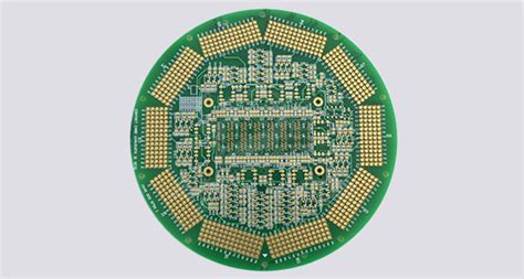
Multilayer PCB Architecture: Powering Advanced Electronic Systems

Key Takeaways
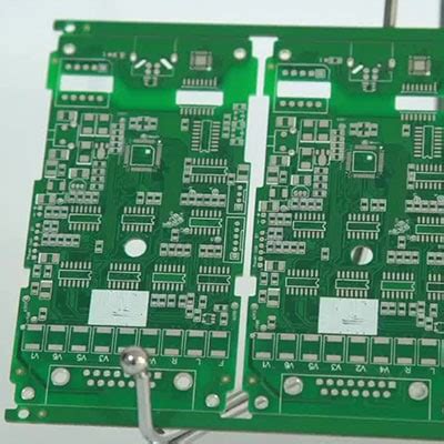
When designing multilayer PCBs, understanding core architectural principles ensures reliable performance in advanced electronics. You’ll need to balance conductive layer integration with high-density interconnect (HDI) technologies to minimize PCB manufacturing cost while maximizing functionality. For instance, collaborating with experienced PCB manufacturing companies helps optimize layer stackup for signal integrity and thermal dissipation.
Tip: Always simulate signal paths early in the design phase to avoid costly revisions during PCB manufacturing business workflows.
Here’s a quick comparison of critical design considerations:
| Factor | Impact on Multilayer PCBs |
|---|---|
| Layer Count | Higher density vs. increased complexity |
| Material Selection | Thermal stability vs. manufacturing cost |
| Via Technology | HDI compatibility vs. fabrication time |
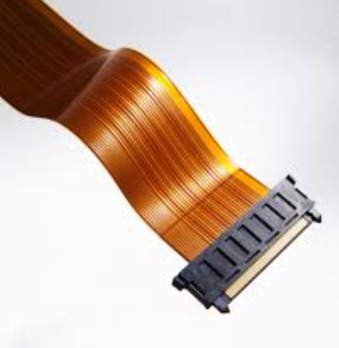
Modern PCB manufacturing relies on advanced materials like low-loss laminates and hybrid dielectrics to reduce crosstalk. For example, using laser-drilled microvias enables tighter interlayer connections, critical for compact designs. Explore advanced PCB solutions here to align your projects with industry benchmarks.
Remember, thermal management strategies—such as embedded copper planes—are non-negotiable in layered architectures. By prioritizing collaboration with PCB manufacturing partners, you ensure scalable solutions that meet both technical and budgetary demands.
Multilayer PCB Stackup Design Essentials
When designing multilayer PCBs, your stackup configuration directly impacts performance, manufacturability, and pcb manufacturing cost. Start by defining the number of conductive layers required for power, ground, and signal routing. A balanced arrangement—such as symmetrical core and prepreg layers—ensures mechanical stability while minimizing warpage during pcb manufacturing. For high-density interconnects, alternating signal and plane layers reduces crosstalk and enhances signal integrity, particularly in high-speed applications.
Material selection plays a pivotal role: low-loss dielectrics like FR-4 or advanced laminates optimize electrical performance, but they also influence pcb manufacturing business decisions due to varying material costs. To manage thermal loads, integrate thermal vias and strategically place copper planes to dissipate heat—a critical consideration for reliability in compact designs.
Collaborate early with pcb manufacturing companies to align your stackup with their fabrication capabilities. For instance, tighter tolerances on dielectric thickness or copper weight may escalate costs, while standardized layer counts can streamline production. Always validate impedance profiles and via structures through simulation tools to avoid costly redesigns. By balancing electrical requirements with pcb manufacturing realities, you create robust, cost-effective architectures that meet modern electronics’ demands.
Conductive Layer Integration Strategies
When planning conductive layer integration, your choices directly influence pcb manufacturing cost and product reliability. Leading pcb manufacturing companies optimize layer alignment by balancing signal density with thermal dissipation requirements, ensuring minimal crosstalk while maintaining efficient heat distribution. You’ll typically alternate power, ground, and signal layers to create controlled impedance paths—a critical step for high-speed applications.
To reduce pcb manufacturing business overhead, consider layer-sharing techniques like combining power and ground planes in adjacent layers. This approach not only streamlines production but also enhances electromagnetic shielding. However, higher layer counts—common in advanced designs—require precise alignment tools, which may increase pcb manufacturing complexity. Partnering with experienced manufacturers ensures proper registration tolerances, preventing misalignment-induced failures.
Material selection further impacts integration success. Low-loss dielectrics and high-ductility copper foils enable thinner layers without compromising conductivity, supporting miniaturization goals. For cost-sensitive projects, standardized stackups offered by pcb manufacturing companies provide a balance between performance and affordability. Always validate via placement and layer transitions during prototyping to avoid signal reflections—a frequent pitfall in multilayer architectures.
By collaborating closely with your pcb manufacturing partner, you can refine layer configurations to match both technical and budgetary constraints, ensuring scalable solutions for evolving electronic systems.
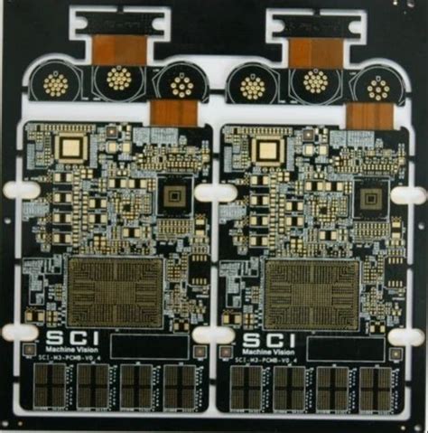
High-Density Interconnect Innovations
To meet the growing demand for compact yet high-performance electronics, PCB manufacturing now prioritizes high-density interconnect (HDI) technologies. These innovations enable PCB manufacturing companies to embed finer traces, microvias, and stacked vias within multilayer boards, reducing overall layer count while boosting functionality. By leveraging laser drilling and advanced photolithography, you can achieve trace widths as narrow as 25 microns—critical for modern devices like wearables and 5G modules.
However, integrating HDI features impacts PCB manufacturing cost due to tighter tolerances and specialized materials. For instance, using low-loss dielectrics or ultra-thin copper foils ensures signal integrity but requires precision equipment. This trade-off challenges PCB manufacturing business models to balance performance with affordability. Transitioning to HDI also demands rigorous testing protocols to prevent defects like microvia cracking or impedance mismatches.
Looking ahead, innovations such as any-layer interconnects and hybrid stacking techniques are redefining design limits. These approaches not only shrink device footprints but also enhance thermal dissipation—a key consideration for next-gen applications. By collaborating with experienced PCB manufacturing companies, you can navigate these complexities while maintaining scalability and reliability in advanced electronic systems.
Signal Integrity Optimization Techniques
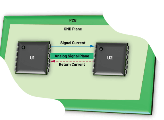
When designing multilayer PCBs, maintaining signal integrity becomes critical as circuit density increases. You can achieve this by implementing controlled impedance traces, which minimize signal reflections and crosstalk between adjacent layers. Leading PCB manufacturing companies often recommend using ground planes adjacent to high-speed signal layers to create a controlled return path, reducing electromagnetic interference (EMI). For instance, via shielding techniques—where ground vias surround sensitive traces—help contain high-frequency noise, a common challenge in PCB manufacturing business environments.
Material selection also plays a pivotal role. Opting for low-loss dielectrics, such as Rogers or Isola substrates, ensures minimal signal attenuation, though this may influence PCB manufacturing cost due to specialized material requirements. Additionally, differential pair routing and precise length matching for critical signals (e.g., clock lines) prevent timing skews in high-speed designs. Advanced PCB manufacturing processes, like laser-drilled microvias, enable tighter trace spacing while preserving signal quality—a necessity for applications like 5G or AI hardware.
To further enhance performance, simulate your design using tools like ANSYS HFSS or Cadence Sigrity before prototyping. These tools identify potential impedance mismatches or resonance issues early, reducing costly revisions. By balancing layer stackup symmetry and minimizing via stubs, you ensure consistent signal propagation across all layers—a cornerstone of reliable multilayer PCB architecture.
Finally, collaborate closely with your PCB manufacturing partner to validate design choices against fabrication capabilities, ensuring manufacturability without compromising electrical performance.
Thermal Management in Layered PCBs
Effective thermal management becomes critical as PCB manufacturing evolves to support higher component densities in multilayer designs. Heat dissipation challenges arise from tightly packed conductive layers and high-speed signal traces, which can generate localized hotspots. To address this, PCB manufacturing companies often integrate thermal vias—plated holes that transfer heat between layers—alongside copper pours or embedded heat sinks. These features balance PCB manufacturing cost with performance, ensuring reliability without overcomplicating production.
When planning your stackup, consider materials with higher thermal conductivity for dielectric layers, such as polyimide or ceramic-filled substrates. These choices reduce thermal resistance while maintaining electrical insulation. Advanced simulations during the design phase help predict heat distribution, allowing you to optimize via placement and layer arrangement. For high-power applications, PCB manufacturing business practices increasingly prioritize hybrid designs, combining traditional FR-4 with metal-core layers for enhanced cooling.
Proactive thermal management not only extends component lifespan but also prevents signal degradation caused by temperature fluctuations. By collaborating with experienced PCB manufacturing partners, you can strike a balance between thermal efficiency, PCB manufacturing cost, and miniaturization goals—key factors in next-generation electronics.
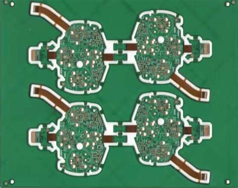
Miniaturization Through Multilayer Architecture
By stacking conductive and insulating layers vertically, multilayer PCBs enable you to achieve significant space savings compared to traditional single- or double-layer designs. This layered approach allows PCB manufacturing companies to embed complex circuitry within a compact footprint, critical for devices like smartphones, wearables, and IoT modules. With high-density interconnect (HDI) technology, traces and vias are miniaturized, reducing the need for bulky wiring while maintaining electrical performance.
However, balancing PCB manufacturing cost with miniaturization goals requires careful planning. Advanced techniques like laser drilling and sequential lamination add precision but increase production complexity. To optimize costs, you must prioritize layer count and material choices—opting for thinner dielectrics or hybrid substrates—without compromising thermal stability or signal integrity.
For PCB manufacturing businesses, this architecture opens opportunities in markets demanding lightweight, high-performance electronics. By integrating power and ground planes into the stackup, you can further shrink board size while shielding sensitive signals. Still, collaboration with fabrication partners is essential to navigate design-for-manufacturability (DFM) challenges, ensuring reliability even as dimensions tighten. The result? Electronics that are not only smaller but also more efficient—a cornerstone of modern innovation.
Advanced Material Selection Guidelines
When designing multilayer PCBs, your material choices directly influence performance, reliability, and pcb manufacturing cost. Start by evaluating thermal stability and dielectric properties—critical for maintaining signal integrity in high-frequency applications. Pcb manufacturing companies often recommend low-loss laminates like Rogers 4350B or Isola FR408HR for impedance-controlled layers, as these materials minimize signal attenuation while supporting high-density interconnects.
For power delivery layers, consider copper weight and substrate thickness. Heavier copper (2-4 oz) improves current-carrying capacity but requires adjustments in etching processes, which impacts pcb manufacturing business workflows. Hybrid stackups combining FR-4 with polyimide cores offer balanced thermal management and flexibility, particularly in aerospace or automotive systems.
Don’t overlook adhesives and prepreg materials—their glass transition temperature (Tg) and coefficient of thermal expansion (CTE) must align with adjacent layers to prevent delamination during thermal cycling. Advanced pcb manufacturing partners typically provide material databases with verified CTE profiles, helping you avoid mismatches in multilayer assemblies.
Finally, collaborate early with fabricators to align material specs with their capabilities. Exotic substrates might promise superior performance but could escalate pcb manufacturing cost by 40-60% compared to standard options. Strategic material selection ensures your design meets technical requirements while remaining economically viable for production.
Future Trends in PCB Layer Technology
As electronics demand higher performance in smaller form factors, PCB manufacturing is evolving to meet these challenges through innovative layer technologies. Emerging trends focus on embedded passives and active components within multilayer stacks, reducing reliance on surface-mounted parts while enhancing signal integrity. PCB manufacturing companies are experimenting with ultra-thin dielectrics and hybrid materials, enabling sub-10µm layer thicknesses for denser interconnects without compromising thermal stability.
Another key development is the integration of 3D-printed circuitry into multilayer designs, allowing pcb manufacturing cost reductions by minimizing drilling and lamination steps. Flexible-rigid architectures are also gaining traction, merging traditional rigid layers with bendable substrates to support wearable and IoT applications. To address pcb manufacturing business challenges, manufacturers are adopting AI-driven design tools that optimize layer stackups for electromagnetic compatibility (EMC) and power distribution—critical for 5G and automotive systems.
You’ll notice a shift toward sustainable materials like halogen-free resins, driven by environmental regulations and lifecycle demands. These advancements not only extend the capabilities of multilayer PCBs but also redefine how engineers balance complexity, reliability, and pcb manufacturing cost in next-gen electronic systems.
Conclusion
As you’ve seen, multilayer PCB architecture plays a pivotal role in enabling today’s advanced electronics by balancing density, performance, and reliability. The intricate layering of conductive and insulating materials allows for high-density interconnects while addressing critical challenges like signal integrity and thermal management. For PCB manufacturing companies, mastering these design principles directly impacts their ability to deliver solutions that meet evolving industry demands—whether in consumer gadgets, aerospace systems, or IoT devices.
When selecting a PCB manufacturing business, you must weigh PCB manufacturing cost against the technical requirements of your project. Advanced materials and precision layer stacking may raise initial expenses, but they often pay dividends in reduced failure rates and longer product lifespans. Innovations in automated production and optimized stackup designs are helping manufacturers balance affordability with performance, ensuring scalable solutions for both prototyping and mass production.
Looking ahead, the push for miniaturization and energy efficiency will continue shaping multilayer PCB development. By partnering with forward-thinking PCB manufacturing experts, you can leverage emerging technologies—from embedded components to advanced substrate materials—to stay ahead in an increasingly competitive landscape. The right architectural choices today will define the electronic systems of tomorrow.
FAQs
How do multilayer PCBs enhance electronic device performance?
By integrating multiple conductive and insulating layers, multilayer PCB architecture enables high-density interconnects and reduces electromagnetic interference. This design supports faster signal transmission and improved power distribution, critical for advanced systems like 5G infrastructure or AI processors.
What factors influence PCB manufacturing cost for multilayer boards?
Costs depend on layer count, material quality (e.g., high-frequency laminates), and precision requirements. PCB manufacturing companies often balance thermal management needs with budget constraints, as additional layers or advanced substrates like FR-4 Hybrid can increase expenses.
Can standard PCB manufacturing processes handle 12+ layer boards?
Yes, but it requires specialized equipment for precise alignment and lamination. Reputable PCB manufacturing businesses use laser drilling and automated optical inspection (AOI) to ensure reliability in ultra-high-layer-count designs, minimizing defects in miniaturized architectures.
How do you ensure signal integrity in multilayer designs?
Optimizing trace routing, using ground planes, and selecting low-loss materials are key. Partnering with experienced PCB manufacturing providers ensures adherence to impedance control standards, reducing signal degradation in high-speed applications.
Explore Professional Multilayer PCB Solutions
For tailored guidance on complex multilayer designs or cost-effective production strategies, please click here: https://www.andwinpcb.com/pcb-manufacturing/.