Multilayer pcb cross section
Understanding The Basics Of Multilayer PCB Cross Section
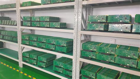
In the realm of modern electronics, the multilayer printed circuit board (PCB) stands as a cornerstone of technological advancement, enabling the compact and efficient design of complex electronic devices. Understanding the basics of a multilayer PCB cross section is essential for those involved in electronics design and manufacturing, as it provides insight into the intricate structure and functionality of these critical components. A multilayer PCB is essentially a stack of multiple single-layer PCBs, each separated by insulating material and interconnected through a series of vias. This configuration allows for a higher density of electronic components and interconnections, facilitating the development of sophisticated electronic systems.
To comprehend the multilayer PCB cross section, one must first appreciate the individual layers that comprise it.
Typically, a multilayer PCB consists of alternating layers of conductive copper and insulating substrate materials. The copper layers serve as the pathways for electrical signals, while the insulating layers, often made from materials such as FR-4, provide structural support and electrical isolation. The number of layers in a multilayer PCB can vary significantly, ranging from as few as four to as many as fifty or more, depending on the complexity and requirements of the application.
The process of constructing a multilayer PCB begins with the fabrication of individual core layers, which are then laminated together under heat and pressure to form a unified structure.
This lamination process is crucial, as it ensures the mechanical stability and electrical integrity of the PCB. During lamination, the layers are aligned precisely to ensure that the vias, which are small holes drilled through the board, connect the appropriate layers. These vias are subsequently plated with copper to establish electrical connections between the different layers, allowing signals to traverse the board vertically.
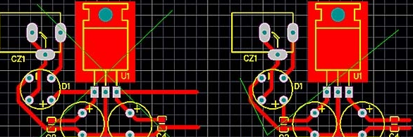
A critical aspect of the multilayer PCB cross section is the arrangement of the layers, which is often referred to as the stack-up.
The stack-up is meticulously designed to optimize the electrical performance of the PCB, taking into consideration factors such as signal integrity, electromagnetic interference, and thermal management. For instance, power and ground planes are typically placed on adjacent layers to minimize inductance and provide a low-impedance path for return currents. Additionally, signal layers are strategically positioned to reduce crosstalk and ensure reliable signal transmission.
The complexity of a multilayer PCB cross section necessitates careful consideration during the design phase.
Designers must account for various parameters, including the thickness of each layer, the dielectric constant of the insulating material, and the width and spacing of the copper traces. These factors influence the electrical characteristics of the PCB, such as impedance and capacitance, which in turn affect the performance of the electronic device.
In conclusion, understanding the basics of a multilayer PCB cross section is fundamental for those engaged in the design and production of electronic devices. The intricate structure of these PCBs, characterized by multiple layers of conductive and insulating materials, enables the creation of compact and efficient electronic systems. By appreciating the nuances of multilayer PCB construction, including the lamination process, via interconnections, and layer stack-up, designers can optimize the performance and reliability of their electronic products, ultimately contributing to the advancement of technology.
Key Benefits Of Multilayer PCB Cross Section In Modern Electronics
In the rapidly evolving landscape of modern electronics, the multilayer printed circuit board (PCB) cross section has emerged as a pivotal component, offering a multitude of benefits that enhance the functionality and efficiency of electronic devices. As technology advances, the demand for more compact, reliable, and high-performance electronic systems has intensified, making the multilayer PCB cross section an indispensable element in the design and manufacturing of contemporary electronic products.
One of the primary advantages of multilayer PCB cross sections is their ability to accommodate complex circuitry within a compact footprint.
By stacking multiple layers of conductive material separated by insulating layers, these PCBs can support a higher density of components and interconnections compared to their single-layer counterparts. This increased density is particularly beneficial in applications where space is at a premium, such as in smartphones, laptops, and other portable devices. The compact nature of multilayer PCBs not only allows for the miniaturization of electronic devices but also contributes to their lightweight design, which is a critical factor in consumer electronics.
Moreover, the multilayer PCB cross section enhances the electrical performance of electronic devices.
The close proximity of the layers allows for shorter signal paths, which in turn reduces signal loss and improves signal integrity. This is especially important in high-frequency applications where maintaining signal quality is crucial. Additionally, the ability to incorporate ground and power planes within the layers helps to minimize electromagnetic interference (EMI) and crosstalk, further ensuring the reliability and performance of the device. These characteristics make multilayer PCBs an ideal choice for applications requiring high-speed data transmission and precise signal processing.
Another significant benefit of multilayer PCB cross sections is their contribution to the durability and reliability of electronic devices.
The layered construction provides inherent structural strength, which enhances the mechanical stability of the PCB. This robustness is essential in applications subjected to harsh environmental conditions or mechanical stress, such as automotive and aerospace industries. Furthermore, the use of advanced materials and manufacturing techniques in multilayer PCBs ensures high thermal performance, allowing them to withstand elevated temperatures without compromising functionality. This thermal resilience is crucial in preventing overheating and ensuring the longevity of electronic components.
In addition to these technical advantages, multilayer PCB cross sections offer economic benefits.
Although the initial design and manufacturing costs may be higher compared to single-layer PCBs, the long-term cost savings are significant. The increased functionality and reliability of multilayer PCBs reduce the need for additional components and complex wiring, leading to lower assembly costs and reduced maintenance requirements. Moreover, the enhanced performance and durability of these PCBs contribute to a longer product lifespan, providing better value for both manufacturers and consumers.
In conclusion, the multilayer PCB cross section plays a vital role in the advancement of modern electronics by offering a range of benefits that address the demands for compactness, performance, and reliability. As electronic devices continue to evolve, the importance of multilayer PCBs in achieving these objectives cannot be overstated. Their ability to integrate complex circuitry, improve electrical performance, enhance durability, and provide economic advantages makes them an essential component in the design and production of cutting-edge electronic systems. As such, the multilayer PCB cross section remains a cornerstone in the development of innovative and efficient electronic solutions.
Design Considerations For Multilayer PCB Cross Section
In the realm of electronic design, the multilayer printed circuit board (PCB) stands as a cornerstone of modern technology, enabling the compact and efficient assembly of complex electronic circuits. A critical aspect of designing these multilayer PCBs is the cross-sectional configuration, which significantly influences the board’s performance, reliability, and manufacturability. Understanding the intricacies of multilayer PCB cross sections is essential for engineers and designers aiming to optimize their designs for both functionality and cost-effectiveness.
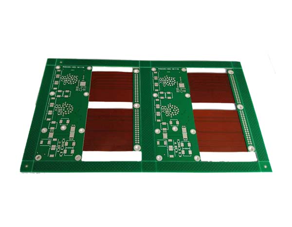
To begin with, the cross section of a multilayer PCB refers to the arrangement and composition of its various layers, including conductive layers, insulating substrates, and any additional materials such as prepregs and solder masks. The number of layers in a PCB can vary widely, from as few as four to as many as fifty or more, depending on the complexity of the circuit and the specific application requirements. Each layer serves a distinct purpose, with some dedicated to signal routing, others to power distribution, and still others to ground planes, which help in reducing electromagnetic interference and improving signal integrity.
One of the primary considerations in designing a multilayer PCB cross section is the selection of materials.
The choice of substrate material, typically a fiberglass-reinforced epoxy known as FR-4, affects the board’s thermal and electrical properties. However, for high-frequency applications, materials with lower dielectric constants and loss tangents, such as Rogers or Teflon-based substrates, may be preferred. Additionally, the thickness of each layer must be carefully determined to balance mechanical strength with electrical performance. Thicker layers can provide better mechanical support but may also increase the board’s overall weight and cost.
Another crucial factor is the arrangement of the layers themselves.
The stack-up configuration, which defines the order and orientation of the layers, plays a pivotal role in the PCB’s electrical characteristics. A well-designed stack-up can minimize crosstalk between signal layers, reduce electromagnetic emissions, and enhance signal integrity. For instance, placing power and ground planes adjacent to each other can create a low-inductance path for return currents, thereby improving the board’s performance in high-speed applications. Moreover, symmetrical stack-ups are often preferred to prevent warping during the manufacturing process, ensuring that the board remains flat and reliable.
Thermal management is also a key consideration in multilayer PCB design
As electronic components become more powerful and compact, the ability to dissipate heat effectively becomes increasingly important. The cross-sectional design can incorporate thermal vias, which are plated holes that facilitate heat transfer from the surface to internal layers or heat sinks. Additionally, selecting materials with high thermal conductivity can aid in managing heat dissipation, thereby enhancing the board’s reliability and longevity.
In conclusion, the design of a multilayer PCB cross section is a complex task that requires careful consideration of various factors, including material selection, layer arrangement, and thermal management. By understanding these elements and their interplay, designers can create PCBs that not only meet the functional requirements of their applications but also adhere to cost and manufacturing constraints. As technology continues to advance, the demand for more sophisticated and efficient multilayer PCBs will only grow, underscoring the importance of mastering the art and science of PCB cross-sectional design.

Common Challenges In Multilayer PCB Cross Section Fabrication
In the realm of electronics manufacturing, multilayer printed circuit boards (PCBs) are indispensable due to their ability to support complex circuitry within a compact form. However, the fabrication of multilayer PCB cross sections presents several challenges that manufacturers must navigate to ensure functionality and reliability. Understanding these challenges is crucial for optimizing production processes and achieving high-quality outcomes.
One of the primary challenges in multilayer PCB cross section fabrication is maintaining precise layer alignment.
As PCBs become more complex, with an increasing number of layers, the potential for misalignment grows. Misalignment can lead to circuit failures, as electrical connections may not properly align between layers. To address this, manufacturers employ advanced registration techniques and equipment to ensure that each layer is accurately positioned. Despite these efforts, achieving perfect alignment remains a persistent challenge, particularly as the industry pushes towards smaller and more densely packed designs.
Another significant challenge is the management of thermal expansion.
Different materials used in PCB construction, such as copper and various substrates, have distinct coefficients of thermal expansion. During the fabrication process, especially during lamination, these materials are subjected to high temperatures. If not properly managed, the differential expansion can cause warping or delamination, compromising the structural integrity of the PCB. Manufacturers must carefully select materials and design PCBs to accommodate these thermal stresses, often employing simulation tools to predict and mitigate potential issues.
Furthermore, the aspect of via formation presents its own set of challenges.
Vias, which are small holes that allow electrical connections between layers, must be precisely drilled and plated. The miniaturization trend in electronics demands smaller vias, which increases the difficulty of ensuring their reliability. Issues such as voids in the plating or misdrilled vias can lead to electrical failures. Advanced drilling techniques, such as laser drilling, and improved plating processes are employed to enhance via quality, yet these solutions also introduce additional complexity and cost.
The fabrication of multilayer PCBs also involves intricate chemical processes, particularly in the etching and plating stages.
These processes must be meticulously controlled to ensure that the desired circuit patterns are accurately formed. Variations in chemical concentrations, temperature, or process timing can lead to defects such as over-etching or under-etching, which can compromise the functionality of the PCB. Manufacturers must implement stringent process controls and continuous monitoring to maintain consistency and quality.
Moreover, as the demand for environmentally friendly manufacturing practices grows, the challenge of managing waste and emissions during PCB fabrication becomes more pronounced. The chemicals used in etching and plating can be hazardous, necessitating careful handling and disposal. Manufacturers are increasingly adopting greener practices, such as using less harmful chemicals and recycling materials, but these initiatives require significant investment and innovation.
In conclusion, the fabrication of multilayer PCB cross sections is fraught with challenges that span from precise layer alignment to environmental considerations. As technology advances and the demand for more compact and efficient electronic devices increases, these challenges are likely to intensify. However, through continuous innovation and the adoption of advanced manufacturing techniques, the industry strives to overcome these obstacles, ensuring that multilayer PCBs continue to meet the evolving needs of modern electronics.