Multilayer pcb cross section
Understanding The Basics Of Multilayer PCB Cross Section
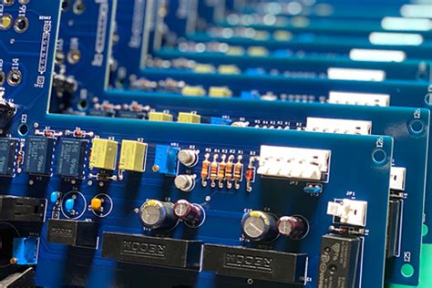
In the realm of modern electronics, multilayer printed circuit boards (PCBs) have become indispensable due to their ability to support complex circuitry within a compact form factor. Understanding the cross section of a multilayer PCB is crucial for engineers and designers who aim to optimize performance, reliability, and manufacturability. A multilayer PCB consists of multiple layers of conductive and insulating materials, which are laminated together to form a single, cohesive unit. This intricate structure allows for the integration of numerous electronic components and interconnections, facilitating the development of advanced electronic devices.
To begin with, the core of a multilayer PCB is typically composed of a dielectric substrate, which provides mechanical support and electrical insulation.
Common materials used for the substrate include FR-4, a glass-reinforced epoxy laminate, and other specialized materials that offer enhanced thermal or electrical properties. The choice of substrate material significantly influences the overall performance of the PCB, as it affects factors such as signal integrity, thermal management, and mechanical stability.
Adjacent to the substrate are the conductive layers, which are usually made of copper.
These layers are etched to create intricate patterns of traces and pads that form the electrical connections between components. The number of conductive layers in a multilayer PCB can vary widely, ranging from as few as four to more than fifty in highly complex designs. The arrangement of these layers is critical, as it determines the routing of signals and the distribution of power throughout the board. To ensure optimal performance, designers must carefully consider factors such as impedance control, crosstalk, and electromagnetic interference when planning the layer stack-up.
Between each pair of conductive layers lies a layer of insulating material known as the prepreg.
This material, which is typically a resin-impregnated fiberglass cloth, serves to bond the conductive layers together while maintaining electrical isolation. The thickness and dielectric properties of the prepreg layers play a vital role in determining the electrical characteristics of the PCB, such as capacitance and signal propagation speed. Consequently, selecting the appropriate prepreg material is essential for achieving the desired electrical performance.
Furthermore, vias are an integral component of multilayer PCBs, providing vertical electrical connections between different layers.
These small, plated holes are strategically placed to facilitate signal routing and power distribution across the board. There are several types of vias, including through-hole vias, blind vias, and buried vias, each offering distinct advantages and trade-offs in terms of manufacturability and electrical performance. The choice of via type and placement is a critical aspect of PCB design, as it can significantly impact signal integrity and overall board reliability.
In addition to the aforementioned elements, the outermost layers of a multilayer PCB are typically coated with a solder mask and a silkscreen layer. The solder mask, usually a polymer-based coating, serves to protect the underlying copper traces from oxidation and accidental solder bridging during assembly. Meanwhile, the silkscreen layer provides essential information such as component labels and reference designators, aiding in the assembly and troubleshooting processes.
In conclusion, understanding the cross section of a multilayer PCB is fundamental for designing and manufacturing high-performance electronic devices. By carefully considering the materials, layer arrangement, and interconnection methods, engineers can optimize the electrical, thermal, and mechanical properties of the PCB, ensuring reliable operation in a wide range of applications. As technology continues to advance, the complexity and capabilities of multilayer PCBs will undoubtedly evolve, further solidifying their role as a cornerstone of modern electronics.
Key Benefits Of Multilayer PCB Cross Section In Modern Electronics
In the rapidly evolving landscape of modern electronics, the multilayer printed circuit board (PCB) cross section has emerged as a pivotal component, offering a multitude of benefits that enhance the functionality and efficiency of electronic devices. As technology advances, the demand for more compact, reliable, and high-performance electronic devices continues to grow, making the multilayer PCB cross section an indispensable element in the design and manufacturing of contemporary electronics.
One of the primary advantages of multilayer PCB cross sections is their ability to accommodate complex circuitry within a compact form factor.
By stacking multiple layers of conductive material separated by insulating layers, these PCBs can support a higher density of components and connections compared to single-layer or double-layer PCBs. This increased density is particularly beneficial in applications where space is at a premium, such as in smartphones, laptops, and other portable devices. Consequently, the compact nature of multilayer PCBs allows for the development of smaller, lighter, and more efficient electronic products, meeting the ever-growing consumer demand for miniaturization.
Moreover, multilayer PCB cross sections offer enhanced electrical performance, which is crucial for the functionality of modern electronic devices.
The close proximity of the layers in a multilayer PCB reduces the length of the electrical paths, thereby minimizing signal loss and improving signal integrity. This is especially important in high-frequency applications, where maintaining signal quality is paramount. Additionally, the ability to incorporate ground and power planes within the layers of a multilayer PCB helps to reduce electromagnetic interference (EMI) and crosstalk between signals, further enhancing the overall performance of the device.
In addition to improved electrical performance, multilayer PCB cross sections contribute to increased reliability and durability of electronic devices.
The layered structure of these PCBs provides greater mechanical strength, reducing the risk of damage from physical stress or environmental factors. This robustness is particularly advantageous in applications where devices are subjected to harsh conditions, such as in automotive or industrial settings. Furthermore, the use of advanced materials and manufacturing techniques in the production of multilayer PCBs ensures high-quality and consistent performance, which is essential for maintaining the reliability of critical electronic systems.
Another significant benefit of multilayer PCB cross sections is their versatility in design and application.
The ability to customize the number of layers and the arrangement of components allows engineers to tailor the PCB to meet specific requirements, whether for consumer electronics, telecommunications, medical devices, or aerospace applications. This flexibility in design not only facilitates innovation but also enables the development of specialized solutions that can address unique challenges in various industries.
In conclusion, the multilayer PCB cross section plays a crucial role in the advancement of modern electronics, offering key benefits that include compactness, enhanced electrical performance, increased reliability, and design versatility. As the demand for more sophisticated and efficient electronic devices continues to rise, the importance of multilayer PCBs in meeting these demands cannot be overstated. By leveraging the advantages of multilayer PCB cross sections, manufacturers and designers can continue to push the boundaries of what is possible in electronic device development, paving the way for future innovations and technological breakthroughs.
Design Considerations For Multilayer PCB Cross Section
In the realm of electronic design, the multilayer printed circuit board (PCB) stands as a cornerstone of modern technology, enabling the compact and efficient assembly of complex electronic circuits. A critical aspect of designing these multilayer PCBs is the cross-sectional configuration, which significantly influences the board’s performance, reliability, and manufacturability. Understanding the design considerations for a multilayer PCB cross section is essential for engineers aiming to optimize their electronic products.
To begin with, the number of layers in a multilayer PCB is a fundamental consideration.
This decision is primarily driven by the complexity of the circuit and the need for signal integrity. More layers allow for additional routing space and can help in managing electromagnetic interference (EMI) by providing dedicated ground and power planes. However, increasing the number of layers also raises the cost and complexity of manufacturing. Therefore, a balance must be struck between the functional requirements and budgetary constraints.
Transitioning to the material selection, the choice of substrate material is another pivotal factor.
The substrate not only provides mechanical support but also affects the electrical performance of the PCB. Common materials include FR-4, a glass-reinforced epoxy laminate, which is widely used due to its good balance of performance and cost. For high-frequency applications, materials with lower dielectric constants and loss tangents, such as PTFE-based laminates, may be preferred. The thermal properties of the substrate are also crucial, especially in applications where heat dissipation is a concern.
Furthermore, the thickness of each layer within the PCB cross section must be carefully considered.
The thickness impacts the board’s overall mechanical strength, impedance control, and thermal management. Thicker boards can handle more current and provide better heat dissipation, but they may also be more challenging to manufacture and less flexible. Conversely, thinner boards are lighter and more suitable for compact devices but may require additional design considerations to ensure adequate performance.
In addition to layer thickness, the arrangement of layers plays a significant role in the PCB’s functionality.
A well-planned stack-up can enhance signal integrity by minimizing crosstalk and ensuring controlled impedance. Typically, signal layers are sandwiched between ground and power planes, which act as reference planes to stabilize the signals. This configuration helps in reducing EMI and improving the overall electromagnetic compatibility (EMC) of the device.
Moreover, the via design is an integral part of the multilayer PCB cross section.
Vias are used to connect different layers electrically, and their design can affect both the electrical performance and the manufacturability of the PCB. Blind and buried vias can save space and reduce parasitic inductance, but they add complexity and cost to the manufacturing process. Therefore, careful consideration must be given to the type and placement of vias to ensure optimal performance without unnecessary expense.
Finally, manufacturability is a crucial consideration in the design of a multilayer PCB cross section.
The design must align with the capabilities of the chosen fabrication process to avoid issues such as warping, misalignment, or incomplete etching. Collaboration with manufacturers during the design phase can help identify potential challenges and ensure that the design is both feasible and cost-effective.
In conclusion, designing a multilayer PCB cross section involves a delicate balance of various factors, including layer count, material selection, layer thickness, stack-up configuration, via design, and manufacturability. By carefully considering these elements, engineers can create PCBs that meet the desired performance criteria while remaining within budgetary and manufacturing constraints.
Common Challenges In Multilayer PCB Cross Section Fabrication
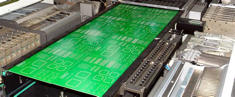
In the realm of electronics manufacturing, multilayer printed circuit boards (PCBs) are indispensable due to their ability to support complex circuitry in a compact form. However, the fabrication of multilayer PCB cross sections presents several challenges that manufacturers must navigate to ensure functionality and reliability. Understanding these challenges is crucial for optimizing production processes and achieving high-quality outcomes.
One of the primary challenges in multilayer PCB cross section fabrication is maintaining precise layer alignment.
As PCBs become more complex, with layers often numbering in the double digits, ensuring that each layer aligns perfectly with the others is critical. Misalignment can lead to circuit failures, as electrical connections may not properly interface between layers. To address this, manufacturers employ advanced registration systems and optical alignment techniques, which help in achieving the necessary precision. Despite these technologies, the process remains sensitive to environmental factors such as temperature and humidity, which can cause materials to expand or contract, further complicating alignment efforts.
Another significant challenge is the management of thermal stresses during the fabrication process.
Multilayer PCBs are subjected to various thermal cycles, particularly during soldering and lamination. These thermal stresses can lead to warping or delamination, where layers separate from one another, compromising the structural integrity of the board. To mitigate these risks, manufacturers must carefully select materials with compatible thermal expansion coefficients and employ controlled cooling processes. Additionally, the use of advanced simulation tools allows for the prediction and management of thermal behavior, reducing the likelihood of defects.
The aspect of via formation also presents a notable challenge in multilayer PCB cross section fabrication.
Vias, which are small holes that allow electrical connections between layers, must be precisely drilled and plated to ensure reliable conductivity. The miniaturization trend in electronics demands increasingly smaller vias, which can be difficult to produce consistently. Laser drilling and advanced plating techniques have been developed to address these challenges, but they require significant investment and expertise. Moreover, ensuring the integrity of these vias is critical, as any defects can lead to open circuits or increased resistance, affecting the overall performance of the PCB.
Material selection is another area where challenges frequently arise.
The choice of substrate materials, copper thickness, and dielectric constants must be carefully considered to meet the specific electrical and mechanical requirements of the application. Incompatibility between materials can lead to issues such as impedance mismatches or signal integrity problems. Manufacturers must balance these considerations with cost constraints, often necessitating trade-offs that can impact the final product’s performance.
Furthermore, the inspection and testing of multilayer PCB cross sections pose their own set of challenges
.Given the complexity and density of these boards, traditional inspection methods may not suffice. Advanced techniques such as X-ray inspection and automated optical inspection (AOI) are employed to detect defects that are not visible to the naked eye. However, these methods can be costly and time-consuming, requiring a careful balance between thoroughness and efficiency.
In conclusion, the fabrication of multilayer PCB cross sections involves navigating a myriad of challenges, from precise layer alignment and thermal stress management to via formation and material selection. Each of these challenges requires careful consideration and advanced technological solutions to ensure the production of reliable and high-performance PCBs. As the demand for more complex and compact electronic devices continues to grow, the ability to effectively address these challenges will remain a critical factor in the success of PCB manufacturers.


